Continue to Site

Welcome to EDAboard.com

Welcome to our site! EDAboard.com is an international Electronics Discussion Forum focused on EDA software, circuits, schematics, books, theory, papers, asic, pld, 8051, DSP, Network, RF, Analog Design, PCB, Service Manuals... and a whole lot more! To participate you need to register. Registration is free. Click here to register now.

Transmission Line Design for GSM Module

Status
Not open for further replies.

ste2006

Advanced Member level 4
Joined
May 1, 2012
Messages
118
Helped
3
Reputation
6
Reaction score
3
Trophy points
1,298
Activity points
2,226
Transmission Line Design Advice for GSM Module???

First of all i know High Frequency PCB Design is a specialist area so please stay with me on this, I am an embedded engineer but need to lay out a PCB for a Telit GL865 GSM Module,

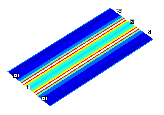
I have gone through the Hardware manual and think it best to stick to what they recommend as works and lay out a Grounded Coplanar Waveguide line on the top layer of my PCB. I am hoping to just use a double sided PCB and use a ground plane on the underside of the board beneath the transmission line on top. (If anyone has any better ideas please tell also)

My question is as follows:

If i use a short a line as possible to the female SMA connector does the actual length of the trace make a difference. I know the width of the trace, height of it, substrate, distance either side etc all are important but on any of the calculators i have used or materials i have read nothing seems to make refernce to the length of trace.

Is this important and if so how does it factor in to the calcualtions??

Secondly i am hoping to avoid using multilayer boards mainly due to cost but if i am using RF like this do i need a complete side of the board as a ground plane or can i get away with just under the module and transmission lines for a ground plane,

I will have to at some stage make sure it complies with EMC Regulations so please keep this in mind also,

Thanks in advance,


Thanks,
 
Last edited:

The trace length matters if no impedance matching is provided. For very short trace l < λ/10 (about 10 mm at 2 GHz) exact trace matching can be ignored, otherwise matching the 50 ohm antenna impedance would be preferred. It's no problem to achieve it either in multilayer or double side PCB.

Here's a same topic thread discussing some layout options (microstrip, coplanar with or without ground) https://www.edaboard.com/threads/233398/

Partial ground plane can work, it's essential to connect ground copper features of both sides through a via fence of sufficient density.
 

Re: Transmission Line Design Advice for GSM Module???

If i use a short a line as possible to the female SMA connector does the actual length of the trace make a difference.

The length makes a difference because longer lines will show "transmission line effects", which you can ignore for very short lines.

Short lines:
The line can be considered short if the length is less than 1/10 wavelength.
For lines in FR4 with effective permittivity of ~4.2...4.7, the effective wavelength is ~2x smaller than in air.

Lines that are not short:
In this case, try to match the line impedance to the source/load impedance (typically 50 ohm).
You could use microstrip line (line above a wide ground) or coplanar line (line at the same layer as the ground, side by side) . Some people also use coplanar over ground, where the co.planar ground strips are connected to the ground below using via fences.

- - - Updated - - -

do i need a complete side of the board as a ground plane or can i get away with just under the module and transmission lines for a ground plane

You need a clean ground for the RF path only. Clean path means that signal and ground path are well defined. For example, there must be no slots/underpaths in the ground underneath the signal line.

Having a larger ground outside the RF section would only be needed if you had a built-in antenna that needs such large ground to operate properly.
 

Re: Transmission Line Design Advice for GSM Module???

The length makes a difference because longer lines will show "transmission line effects", which you can ignore for very short lines.

Short lines:
The line can be considered short if the length is less than 1/10 wavelength.
For lines in FR4 with effective permittivity of ~4.2...4.7, the effective wavelength is ~2x smaller than in air.

So am i correct in saying short is less than about 8.8mm??

Lines that are not short:
In this case, try to match the line impedance to the source/load impedance (typically 50 ohm).
You could use microstrip line (line above a wide ground) or coplanar line (line at the same layer as the ground, side by side) . Some people also use coplanar over ground, where the co.planar ground strips are connected to the ground below using via fences.

So if i use a Coplanar line then i do not need a ground below the antenna trace?? Or maybe just a small segment of ground??

I have read the other topic already before posting but just did not get a final conclusion from it hence the new post,

Thanks,
 

Re: Transmission Line Design Advice for GSM Module???

So am i correct in saying short is less than about 8.8mm??

What frequency did you calculate for?

Let's do something approximate:
f=2 GHz
wavelength in air = 3e8m/s / 1GHz = 150mm
1/10 wavelength in air = 15mm
1/10 wavelength inside FR4 = 15mm / SQRT(4) = 7.5 mm

If the line is shorter than this, transmission line effects are small and you don't need to apply transmission line concepts / matched impedandce lines.

So if i use a Coplanar line then i do not need a ground below the antenna trace?? Or maybe just a small segment of ground??

If you use controlled impedance lines, this means that you control the ratio of series L and shunt C of the transmission line. You can do so by using microstrip or coplanar configuration. Coplanar means that you don't need a ground below, and instead use a ground "on the side".

The disadvantage of microstrip (=ground below) for FR4 with 1.5mm thickness is that the distance (and thus shunt capacitance) is determined by the 1.5mm substrate height, and you need a really wide line (~2.7mm) to achieve the required L/C ratio for 50 ohm line impedance. If you use other configurations, you might be able to increase the capacitance between signal and ground of the line, and achieve 50 ohm line impedance with a narrower line width.
 

Re: Transmission Line Design Advice for GSM Module???

ok starting to make sense now,

Any benefit to a Grounded Coplanar Waveguide Vs a regular Coplanar Waveguide??

Ill start to do some maths then and come back to you guys once i have some numbers :)

- - - Updated - - -

ok i have done some maths as follows and would appreciate any thoughts or opinions,

Ideally i would like to keep the trace length below 7.5mm or so but im not sure how realistic this is (BTW i did my claculations based on 1.8Ghz)

Failing a super short trace maybe i could try a Coplanar WaveGuide on the top side of the board,

If i go with: relative permitivity of FR4 @ 4.6, trace width of 1.5mm, Ground Plane Spacing of 0.2mm and board thickness of 1.6mm i am getting 51.2 ohm impedance which i think is ok??


2mm| 0.2| 1.6mm| 0.2| 2mm
------_____----------___----------
1.6mm Substrate (FR4)
_____________________________

I do not plan on having ground planes where i can expcept around the microcontroller crystal and small places where necessary,

Plan would be to just tie the Groound traces to Ground,

Anyone any thoughts??

Thanks,
 

Re: Transmission Line Design Advice for GSM Module???

If i go with: relative permitivity of FR4 @ 4.6, trace width of 1.5mm, Ground Plane Spacing of 0.2mm and board thickness of 1.6mm i am getting 51.2 ohm impedance which i think is ok??

Yes, this is fine. I double checked with my EM tool (Sonnet) which gives me ~52 Ohm.

Any benefit to a Grounded Coplanar Waveguide Vs a regular Coplanar Waveguide??

One reason to have a ground below is that you might need that backside ground in the circuit anyway. For the line itself, there is no real advantage. The line would be a little bit narrower, and the fields a little bit better shielded. But the shielding with coplanar ground strips at 0.2mm distance is already excellent.


Plan would be to just tie the Groound traces to Ground

Yes. Just make sure to connect (bridge) both grounds strips at each end of the line, so that ground current will flow through both ground strips.
 

Re: Transmission Line Design Advice for GSM Module???

Yes. Just make sure to connect (bridge) both grounds strips at each end of the line, so that ground current will flow through both ground strips.

You just mean basically create a loop with the ground strips encircling the transmission line is it??

Any problems then with length of the transmission trace, within reason obviously, Have i read about keeping it less than one wavelength and not finishing it on a half or quarter and things like that??

Thanks,
 

Any problems then with length of the transmission trace, within reason obviously, Have i read about keeping it less than one wavelength and not finishing it on a half or quarter and things like that??
As said, you don't need to think about resonating length for a matched transmission line. A FR4 transmission line will involve some dielectric losses, also all open TL structures are radiating to a certain extend. You don't want to make it longer than needed.

create a loop with the ground strips encircling the transmission line is it??
Continuous ground at both sides is at least a minimal requirement. An ideal coplanar wave guide (CPW) would have infinite ground at both sides. Reducing the ground to small "strips" will create a kind of differential transmission line where the ground becomes also "hot" and couples to the surrounding circuit. If the room for the transmission line is very restricted, a ground plane below it and via fences for the coplanar ground strips would be better.
 
Last edited:

Continuous ground at both sides is at least a minimal requirement. An ideal coplanar wave guide (CPW) would have infinite ground at both sides. Reducing the ground to small "strips" will create a kind of differential transmission line where the ground becomes also "hot" and couples to the surrounding circuit.

Below is a visualization of the currents at 1.8GHz for the given dimensions. The current/field rapidly decreases as we move away from the narrow slot. There is not much value in using wider ground strip in this case.


100% agreed on the other aspects. Having a matched line means that length is not critical. The rules with wavelength dependency apply for lines that are not matched.
 

Below is a visualization of the currents at 1.8GHz for the given dimensions. The current/field rapidly decreases as we move away from the narrow slot. There is not much value in using wider ground strip in this case.
Thanks for the clarification. I also had the idea that the field behind the ground strips should almost cancel, similar to a coaxial line.

I think however, we should be careful to conclude from the results of an ideal coplanar line to less symmetrical cases, e.g. a coplanar line with a bend. It's more than superstition when RF designer use to place via fences in similar situations.
 

I think however, we should be careful to conclude from the results of an ideal coplanar line to less symmetrical cases, e.g. a coplanar line with a bend.

100% agreed! At bends and other discontinuities, it's good design practice to add some underpass/connection between the grounds, to keep both ground strips at the same voltage.

It's more than superstition when RF designer use to place via fences in similar situations.

I don't want to argue against bottom ground metal, and via fence to connect all those ground together. Such grounded coplanar line is less popular among RF designers, but it can be used. In general, the line dimensions need to be re-calculated when adding the bottom ground and via fences. I checked that with an EM simulator: For this particular case, with 1.6mm substrate thickness and 0.2mm gap width, the effect of the bottom ground on line impedance is small, and the 1.6mm line width can be used for both cases.
 

Status
Not open for further replies.

Part and Inventory Search

Welcome to EDABoard.com

Sponsor

Back
Top