shash
Junior Member level 2
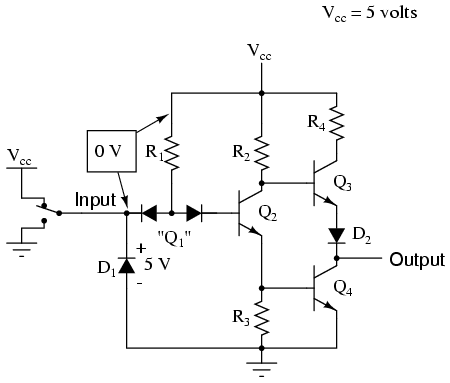
hey guyz,in the diagram there is ttl not gate given.i wanted to know in which configuration(CB,CE,CC) is the transistor Q2 connected and how to determine that.
Follow along with the video below to see how to install our site as a web app on your home screen.
Note: This feature may not be available in some browsers.
")
..............
sir if that is true then in case of CC the collector isnt connected to ground.In the diagram the ouput is taken from emitter(for Q4) as well as collector(for Q3)
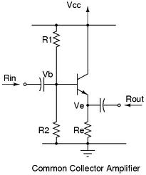
Mr. Brian,Consider that as far as the signal is concerned the Vcc and Ground are at the same potential. Obviously this is not true for the DC conditions or it wouldn't work. So in that schematic it would be classed as "common collector" although the more common name is "emitter follower", particularly if you add a resistor in the collector line.
Brian.
How to Determine Configuration of Transistor Circuit
The best way to characterize the configuration of a BJ transistor circuit is to determine the input and output leads. The remaining lead is the common lead.
Clearly in your example, the base is the input and the emitter is the output. Hence it is CC. Using a collector resistor will not change this.
In the initial circuit of the thread, Q2 is has two outputs. However, only one of the two outputs are of importance at any given time, depending on the logical state of the Q2 switch. When the switch is on, it is used as CC and when the switch is off it is used as CE.
Quote Originally Posted by betwixt View Post
Consider that as far as the signal is concerned the Vcc and Ground are at the same potential. Obviously this is not true for the DC conditions or it wouldn't work. So in that schematic it would be classed as "common collector" although the more common name is "emitter follower", particularly if you add a resistor in the collector line.
Brian.
Voltage sources have internal impedances tending to zero ohms. For signal analysis all voltage sources are considered to be short circuits.What does its mean as far as the signal is concerned the Vcc and Ground are at the same potential ... Could you please share some more detail
No it won't.CE configuration will produce a phase difference of 180 degrees between Input and Output
Although the phase hasn't been shifted, an inverter "produces" a phase difference of 180 degree. You can argue about using more instructive terms, but not about the fact. The term difference doesn't imply a particular method how it's been generated."CE configuration will produce a phase difference of 180 degrees between Input and Output"
No it won't.
The signal at the collector is inverted with respect to the emitter. There is no phase shift.
The two parts of your sentence are contradictory.Although the phase hasn't been shifted, an inverter "produces" a phase difference of 180 degree.
The fact is that there is no phase shift, there is no phase difference.... about the fact.