Continue to Site

Welcome to EDAboard.com

Welcome to our site! EDAboard.com is an international Electronics Discussion Forum focused on EDA software, circuits, schematics, books, theory, papers, asic, pld, 8051, DSP, Network, RF, Analog Design, PCB, Service Manuals... and a whole lot more! To participate you need to register. Registration is free. Click here to register now.

Basic question on capacitotrs in Spectre

Status
Not open for further replies.

Ravinder487

Full Member level 3
Joined
Jul 9, 2010
Messages
169
Helped
0
Reputation
0
Reaction score
0
Trophy points
1,296
Location
Bangalore, India
Activity points
2,469
Basic question on capacitors in Spectre

Hi,
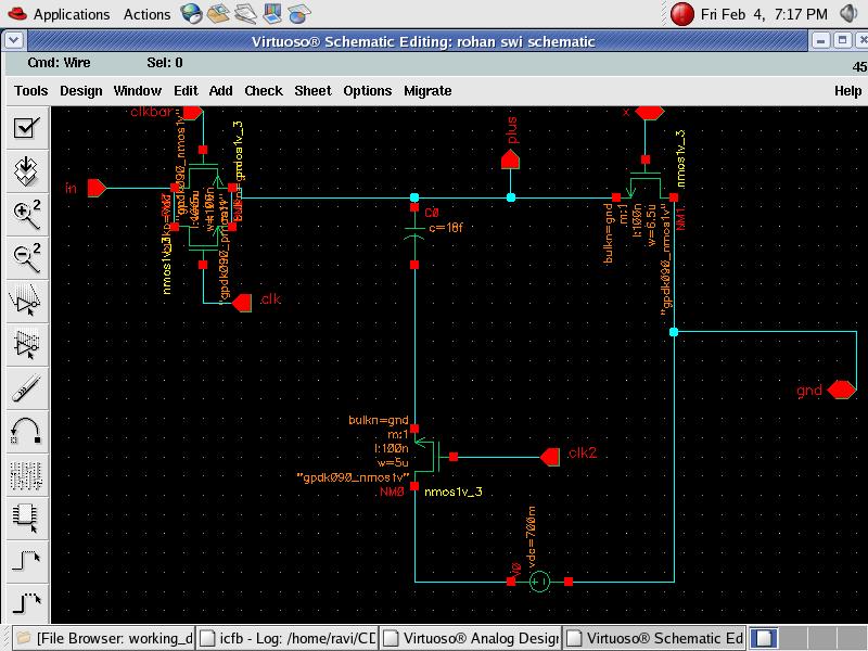
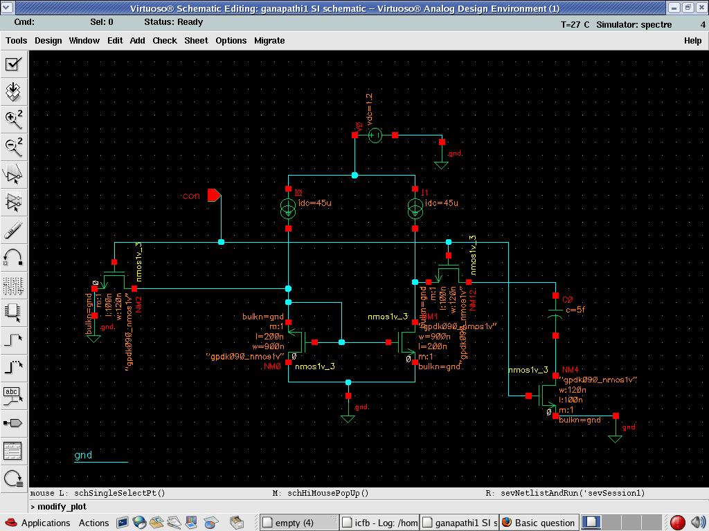
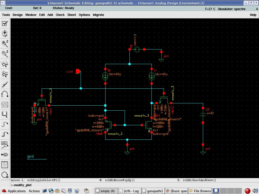
I find lot of capacitances in Spectre.Two of them are "cap" in "analogLib" and "nmoscap" in gpdk090.what is the difference between these two.
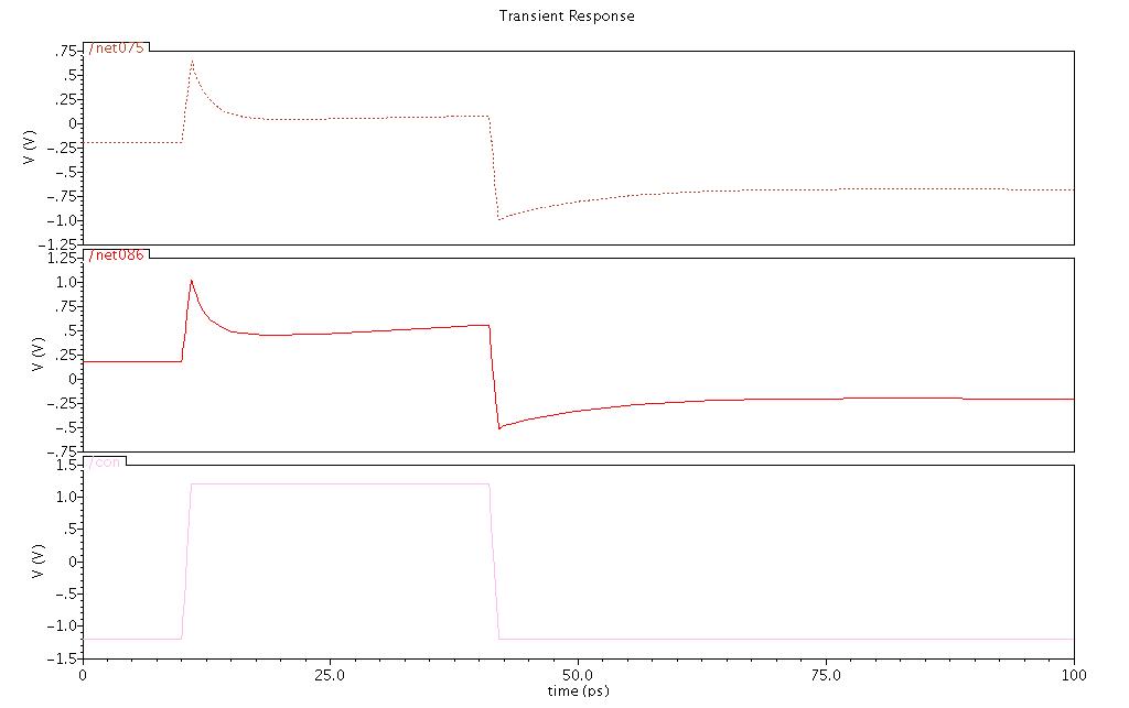
If I simulate using "cap" it is taking too much of time to charge(around 20ps) and with nmos cap it is <1ps.why is it so.
In the paper I'm referring author has used capacitor formed by three metals(M3 M4 M5).what is the equivalent capacitor in Spectre.
And one last questions what type of capacitors are used in actual ADC and WHY!!?
Thanks&Regards,
Ravinder Jakkidi.
 
Last edited:

Hi all ,I'm facing lot of problems with capacitor in Spectre .I don't know why the terminals of capacitor are charging neither to Vdd nor to -Vdd when I'm using a pass transistor to drive the capacitor. If anybody has faced similar problem please help me in figuring out the error that I'm making in my connections.
Till now I've posted three threads in this forum but I didn't get any replies.Experienced guys in the forum please guide beginners like me..
Thanks&Regards ,
Ravinder.
 

Till now I've posted three threads in this forum but I didn't get any replies.

This should trigger some thoughts about: why?
Did you, possibly, forget to post schematics in order to explain your questions?
 

Hi Erikl,
Actually all of my posts seems to be more general than specific to that circuit.So I've carefully defined the problem statement in a generalized way and I had thought to post schematics at later time in discussion.But none participated in the discusion.
Coming to current issue I'm posting schematic and output of the circuit.Please help me in solving the problem.

Thanks &Regards,
Ravinder.
 

I do not know the exact model of the nmos cap, but I guess it follows the operating regions of a typical MOS cap.
**broken link removed**
The cap in analogLib is an ideal capacitor, ie no voltage dependence, no leakage, no ESR etc.
The author of the paper you are referring to is likely using a MIM or MOM cap. What cap to use depends on your requirements. You should refer to your process documentation on figures like leakage, matching coefficients, any biasing requirements, voltage dependence/limits and cap per area etc.
 
Last edited:

cap in analogLib is an ideally cap with default value of 1pF. cap in gpdk090 should be cap from some special process. And moscap is voltage dependent. cap value will be very small when its voltage is close to vth. So it leads to faster charging.
 

Can u plz explain me what is that happenning in my circuit

"net075" and "net085" are voltgaes at two terminals of the capacitor.I don't why votage at the terminals are rising eventhough there is no closed path for the terminals to get charged up ( "con" signal is turning of the transistors "NM12" and "NM4").
And if I removed "NM4" voltage at top of capacitor is stable.

Please help me,its urgent.Thanks in advance.
 

When NM4 is turned off, there is no way to keep the voltage at the cap bottom zero. This node will be easily coupled to other voltage by parasite capacitance.
If you want the voltage at the cap bottom to be zero always, it should be shorted to ground.
 

    V

    Points: 2
    Helpful Answer Positive Rating
Then how can I float bottom plate of the capacitor as this very much important in implementing charge redristribution DAC.
 

Whenever you have nodes of very high impedance in your circuit, small stray currents can result in large voltage variations. It's simply V=IZ.
What you are seeing are all the non-idealities faced by switched cap circuits, clock feedthrough, charge injection, leakage current, parasitic cap etc etc. Take a lesson from switch cap techniques, ie use dummy mos caps, use non-overlapping switching, maybe even control the slew of your control signal. And if that cap is going to float for too long, do not expect it to retain its charges indefinitely.

Added : Just saw your cap is only 5fF. That is on the same order, or maybe even an order lower than stray capacitances. What do you expect?
 
Last edited:

    V

    Points: 2
    Helpful Answer Positive Rating
Thanks for your reply.I think dummy transistor is used to decrease clock-feed through,correct me if I'm wrong.Then what is the possible solution to float bottom plate.If any had experience with charge redristribution DAC please give me some suggestions as drop in potential is very much rapid.
If I increase capacitance then it will take too much time in charging the capacitor.
 

What can be input voltage range that an ADC should be able operate i.e., if in 90nm technology vdd is 1.2 then should the Full Scale Voltage be 1.2V for that ADC.Because my ADC works only for voltage range from 335m to 660m.
Can any body suggest me good papers on Charge Redistribution DAC and Switches used in high Speed DAC.
 

Your bottleneck is probably in the switch drivers. Other than using transmission gate switches, another popular technique is to use bootstrap caps to provide higher driving voltages. I'm a bit skeptical with these techniques on the speed they can provide, and on device reliability with the higher voltages.
 

@Checkmate:If u have any reading material on bootstrap cap circuits can u plz post here.Actually I need only charge redistribution DAC,if u have any good papers on this type of DAC please suggest ...thanks..
 

A quick google of bootstrap gives many articles.
I just grabbed this one.

http://www.eecg.toronto.edu/~kphang/papers/2001/jwong_SH.pdf

It also gives another technique, which is using opamp as a voltage buffer to do away with the switch. This may have bandwidth limitations, and is extremely expensive, but it probably is the only one that gives the widest swing.

You can find a lot of bootstrapping circuits, the basic idea is all the same, charge the cap when switch is off, and drive the switch off the cap. But as I said, use them at your own discretion.
 

Can u give a rough estimation of input swing for 90nm(@vdd=1.2) and operating at speed of 500MSPS
 

Input swing is dependent on your design. It depends on whether you can drive your switches into the linear region. It depends if your opamps can be designed for wide-swing.
As for 500MSPS, that's a pretty steep task, especially for charge redistribution (one of the slowest types of DAC), and probably on the higher end of currently commercially available DACs.
Just imagine how many clocks you need to get a sample out, you are actually working in the GHz range, highly unrealistic.
Most such DACs use multi-channel to provide such sampling rates, and use resistor or current steering topologies.
 
Can u plz read this PDF and suggest any good DAC.To me it seems that charge redistribution DAC well suits for this ADC.
 

@checkmate:I've heard of current steering DAC but I don't basic operation of it .Can u please post some reading material and good papers on design of 6 bit DAC.
I've tried searching in Google but couldn't find any useful stuff.Authors of most papers directly dealt with issues in DAC rather than explaining its operation.
 

Status
Not open for further replies.

Part and Inventory Search

Welcome to EDABoard.com

Sponsor

Back
Top