Continue to Site

Welcome to EDAboard.com

Welcome to our site! EDAboard.com is an international Electronics Discussion Forum focused on EDA software, circuits, schematics, books, theory, papers, asic, pld, 8051, DSP, Network, RF, Analog Design, PCB, Service Manuals... and a whole lot more! To participate you need to register. Registration is free. Click here to register now.

2 stage Amplifier CC-CE

Status
Not open for further replies.

Amondesire

Newbie level 4
Joined
Dec 17, 2016
Messages
6
Helped
0
Reputation
0
Reaction score
0
Trophy points
1
Activity points
50
hi guys, I want to design a two stage Amplifier with the following parameters Av=300, Zi=1M, VCC=+12v I tried deriving the parameters to use but have not been successful as my lecturer has always said I'm wrong. he said its has to be CC-CE which I'm a little bit confused. I wud be greatful someone can help me whatever way you can.
thnks
 

Are there any more specifications?
What is the minimum load value allowed on the output?
Are you limited to one active device per stage?
What is the maximum output swing expected?
Maximum output distortion allowed?
Frequency bandwidth of operation?

- - - Updated - - -

It would be much easier if you were allowed to use a jfet to meet input impedance requirement.

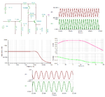
This specific design below performs well, and distortion is just below 2% THD for a 6 Vp-p output swing.
 

Attachments

  • 50dB_amp.png
    50dB_amp.png
    64.3 KB · Views: 116
A CE has an input Z that is a lot less than 1M ohms. But a CC can easily produce an input Z of 1M which is why it was suggested.
The CC can feed a CE which can produce a voltage gain of 300 if it is allowed to have high distortion (no negative feedback).
 

The input impedance of the 2nd stage will have to be high enough as not to load the output of the first stage, as that will reduce the overall input impedance. If you manage to design a 2nd stage with high enough input impedance, the resulting values may prevent you to get the necessary gain required.

Without T2 base connected, the input impedance is near 1M, but as soon as the base is connected the input impedance drops drastically. Making the base bias resistors of T2 larger produces very little difference and gain suffers as well.

Using the jfet eliminates these problems.
 

Attachments

  • 50dB_bip_amp.png
    50dB_bip_amp.png
    61.8 KB · Views: 101

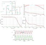
If you use some advanced techniques, you can get the required input impedance (over a small bandwidth) with good gain and acceptable distortion. I am sure this is beyond the scope of this assignment problem.

The design below will have 1M input impedance for something like the speech band (300-3k Hz).
 

Attachments

  • 50dB_bip_amp_hiz.png
    50dB_bip_amp_hiz.png
    55.8 KB · Views: 95

I was told to use a BJT transistor and generate the minimum and maximum load, output swing and distortion. Also find the Q-point and hfe
 

Maybe you should discuss with your professor that the design specifications can't be met by using standard textbook CC and CE stages. The input impedance appears to be a problem and reaching 50 dB gain is another problem, as shown in my simulations.
 

If you use some advanced techniques, you can get the required input impedance (over a small bandwidth) with good gain and acceptable distortion. I am sure this is beyond the scope of this assignment problem.

The design below will have 1M input impedance for something like the speech band (300-3k Hz).

Sir' i would love to know this advanced techniques maybe i could apply it to surprise my supervisor
 

in designing my 2 stage amplifier where I'm expected by my lecturer to use a CC-CE stage which I understand. but I don't know how to;

1. get the values that are required in the CC stage to give a 1M0 input impedance.
2. work out what values in the CE stage that are required to give a voltage amplification of 300
3. the Q-points and the calculation

I'm still new to Electronics system I need help
Thnks
 

Hi,

"Analog Design Essentials" - W Sansen

"Analysis and Design of Analog Integrated Circuits" - Gray, Meyer, et al

"Modern Techniques for the Design of BJT OP Amps" by Sedra in his Microelectronic Circuits (chapter 13)

I couldn't do the calculations for you, but having found the first book myself, and followed recommendations of EDA members in other similar/related posts to read the other two books, I believe that if you search these books for the formulas you need you will be able to begin to answer your own questions quicker than you might think. Even so, I hope some-one else is able to give you a more useful answer for the time being.

As far as I recollect, the formulas, "simplified" models, etc., and examples are in the second book, and introduced in the first in the list; both discuss calculating input impedance and gain for different architectures, and both definitely analyse two-stage amplifiers (both BJT and MOS).

It might be nice to know if you are expected to invent the transistors based on the requirements or use mass-produced devices.

Good luck!

Sorry I can't be of more help.
 

Status
Not open for further replies.

Part and Inventory Search

Welcome to EDABoard.com

Sponsor

Back
Top