Continue to Site

Welcome to EDAboard.com

Welcome to our site! EDAboard.com is an international Electronics Discussion Forum focused on EDA software, circuits, schematics, books, theory, papers, asic, pld, 8051, DSP, Network, RF, Analog Design, PCB, Service Manuals... and a whole lot more! To participate you need to register. Registration is free. Click here to register now.

13.56Mhz Class E Power Amplifier for Plasma Generation

Status
Not open for further replies.

keathow87

Junior Member level 1
Joined
Feb 6, 2011
Messages
15
Helped
0
Reputation
0
Reaction score
0
Trophy points
1,281
Activity points
1,419
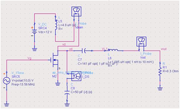
hi, friends...I'm currently working on my Final Year Project to construct a plasma needle and facing problems in construct my RF supply. I'm using MOSFET IRF540N in my circuit as switching device and got some question here:

1) Does this IRF540N actually require Vgs of 15V to on/off it instead of the 2.5V shown in the datasheet?

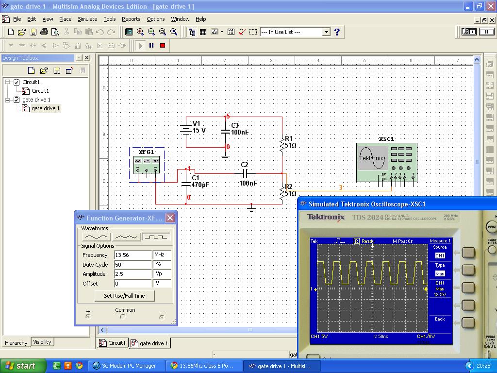
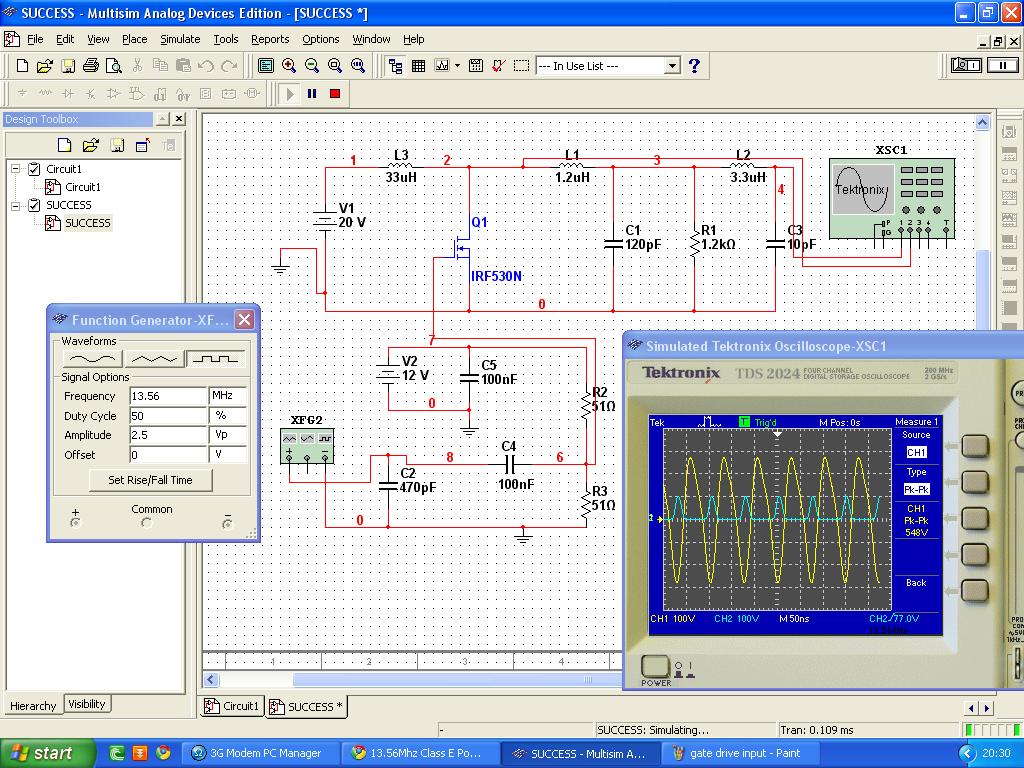
2) The current instrument available for me only manage to provide a 13.56Mhz, Vpp of 2.5V square wave to my MOSFET, and it is a function generator. Is it possible for me to amplify the signal to Vpp of 15V?? what circuit needed to do it??

3) Any gate drive circuit available to provide a Vpp 15V, 13.56Mhz square wave if it is impossible to amplify the signal from function generator?

I'm really in need of your kind help and run out of time, so please help me:sad:
 

Class E is a realistic approach and should work with standard MOSFET as IRF540. There are however special devices dedicated to MHz switching, e.g. from IXYS. Class E doesn't imply "square wave" input, just a certain degree of input overload. At higher frequencies, it's mostly a sine waveform.

10 ns order of magnitude risetimes can be achieved with standard gate drivers. But unfortunately, they won't stand the power dissipation with 13 MHz switching frequency. So you most likely need to assemble the gate driver from discrete components. The design is basically simple: Define the intended rise and fall time, calculate the necessary gate current, select suitable transistors.
 
dear FvM, thank you so much for the reply.

So is that mean i should replace my MOSFET with IRF540? sorry but i'm totally new and have no idea in circuit design. The circuit I'm using now is just a modified version from a paper i read but I failed to get the desired output and I think gate driving is the main prob.

1) Define the intended rise and fall time<<<from what i know, i need to have a 13.56Mhz, duty ratio 50%, Vpp of 15V input for my MOSFET but i have no idea of how the gate driving circuit looks like, can you provide any standard circuit for me???

2) calculate the necessary gate current<<<so what should I concern is gate current but not gate voltage??

3) select suitable transistors<<<Does it mean IRF540N not suitable??
 

I didn't mean IRF540 instead IRF540N, they are just the same, N is for RoHS (lead-free solder) version. What's the suggested gate drive in your paper?

Theoretically, you could drive the FET with a few volts around the threshold voltage. But in practice, the package has a considerable source inductance that causes a voltage drop.

As I already mentioned, the standard class E approach would be sine wave input and a LC matching network at the gate. Although the efficiency will be possibly a few percent lower than with optimized switching gate drive, it's much easier.
 

94_1287472044.jpg

hmm, maybe i should state my problem like this>>>>the connection i using now is basically the same with this circuit, but the main problem is i don't have any equipment to provide the source for Vg as in SRC5 which is V=polar(10V) with 13.56Mhz frequency.

1) All I got now is a function generator that can provide Vpp of 2.5V and I'm planning to amplify it to 15V, is it possible?

2) There is no suggested gate drive in the paper @.@ So i seriously don't know how does it looks like...

By the way, thanks for your explanation...I was still wonder why the Vpp of 2.5V do well in my simulation but it failed when come to practical = = I knew I'm the kind of really slow in learning, hope you won't mind to keep teaching me, thanks =)
 

https://obrazki.elektroda.pl/28_1297149430.jpg
this is the ideal output i want to get, the MOSFET available in this simulation is IRF530N. However, the input from XFG1 is only a 13.56Mhz, 2.5Vp square wave and it works perfectly well. Why it comes to a problem when test in real practice?


https://obrazki.elektroda.pl/42_1297149430.jpg
btw, i tried to amplify the voltage from the output of function generator and that's what i get. I was manage to amplify it from Vp of 2.5V to 10V now but it's still useless when come to connect the C2 to the gate of MOSFET. Can any1 tell me why it failed??
 

Without reasonable DC bias, neither 2.5 nor 10Vpp will work. AC coupling without a bias network is a bad idea. With a bias, you should a least get some output. Of cause you have to care, that the DC drain current doesn't cause too much dissipation. Why don't you show the gate waveforms?
 

I would expect an offset voltage set for the generator.
 

offset voltage? i had never come to know what is the use of it...does it make any difference in real practice? what value should I set?
 

Check the gate drain current versus gate voltage characteristic of your MOSFET and consider what you're doing.
 

Alright, I'm not sure is it a good news or bad news. My instructor finally agreed to buy some component for my project, but the budget can not be too high. 2 things i need now are IXYS RF-DEIC420-IC,DRIVER,MOSFET DE275 and IXYS RF DE275-501N16A, if I can only choose one, which one is most needed in my project?

1) Is it possible to generate the plasma by using the DEIC420 to drive the IRF540N MOSFET? i heard that a RF MOSFET like DE275 series is more suitable in generating plasma but the problem is out of budget. The MOSFET is even expensive than the MOSFET driver...any suggestion please?? thank you...
 

Is it possible to generate the plasma by using the DEIC420 to drive the IRF540N MOSFET?
I don't remember that you told an intended output power, which would obviously depend on the involved plasma source. So how can we know?
 

sorry for the lack of information given:sad:

btw, FvM...can you please show me how to use the MOSFET as switching device?? I had connected the circuit as shown in the simulation but the output is really low. My Instructor told me that maybe i haven't even able to turn ON/OFF the MOSFET.

So is there anyway i can know my MOSFET is on or off? Can you please provide me any circuit that can be use to switching the MOSFET?? again, the MOSFET is IRF540N. All I got is a function generator but it can only output a 2.5Vp square-wave:sad: so I can't drive the MOSFET like the others do simply with a function generator....
 

Usually, fast switching is done with a square wave at the gate, driven by a low impedance (e.g. 5 to 10 ohm, maximum 50 ohm) source, with voltage levels of 0 (off) and 10 to 15V (on). This can be read from any power MOSFET datasheet, I think.

In class E operation, one would simply apply a sine voltage, possibly distorted by a preamplifier. A DC bias can be used to adjust the duty cyle. The main advantage of a sine voltage is, that it can use LC impedance matching circuits to effectively eleminate the gate capacitance and increase the drive level to the gate. Sine wave drive is the only option at higher frequencies.

13.56 MHz would generally allow some kind of switching operation, with trapezoidal gate and output waveforms, but requiring strong gate drive circuits. Your function generator, except for having limited output voltage, most likely hasn't sufficient low output impedance.

I suggested more than once to try with the function generator, adding a DC offset to raise the gate voltage above the threshold level. I'm not sure if you even tried.
 
Thanks for the explanation =) but i doubt that is it possible to effectively switch the mosfet if i got a 2.3V to 13.2V square wave?? This is because i somehow manage to find a circuit that can provide that square wave and when i combine it with my class E power amp, its WORK!!!

This is the input signal
63_1297600376.jpg


and when combined
47_1297600376.jpg


Will this circuit work?? i doubt that because before this i manage to get the same output just by applying signal from function generator but failed in real work...sorry but i just figured out what is offset voltage function, will try it together with this circuit on next Wed after my test, thank you...
 

One would want to know the output impedance of the real function generator. The bias voltage network must not be necessary of that low resistance, because the gate is not consuming DC current. The other option would be to build a sufficient fast driver. But I don't know, which electronic devices are availiable to you.
 

means that i have to try it on real circuit only know it work or not since I don't know the output impedance of the real function generator?

alright, then i just change it to 500ohm...

hmm, can you provide the schematic 1st?? I'll try my best to get all electronics needed...thank you =)
 

I don't know the output impedance of the real function generator
If it's standard lab instrument, it should have a specification. Most likely, the output impedance is 50 ohm.

The bias voltage should be adjustable, either by varying the voltage source or using a potentiometer.
 

Status
Not open for further replies.

Part and Inventory Search

Welcome to EDABoard.com

Sponsor

Back
Top