Continue to Site

Welcome to EDAboard.com

Welcome to our site! EDAboard.com is an international Electronics Discussion Forum focused on EDA software, circuits, schematics, books, theory, papers, asic, pld, 8051, DSP, Network, RF, Analog Design, PCB, Service Manuals... and a whole lot more! To participate you need to register. Registration is free. Click here to register now.

Transistor biasing problem

Status
Not open for further replies.

tictac

Full Member level 5
Joined
Oct 22, 2006
Messages
297
Helped
3
Reputation
6
Reaction score
3
Trophy points
1,298
Location
Polland
Activity points
3,572
Hi
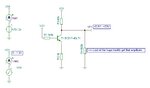
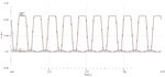
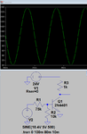
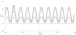
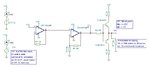
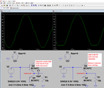
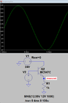
I have a transistor that work at active mode . The base input of the transistor is about 0 to 10 volts. The collector is connected to the 24 volts.The emiter output is about 0.5 volts to 9.5 volts.
But I want that the emiter output is changing form 0 to 24 volts. The current of this voltage is about 100mA.
How can I change my circuit for changing from 0 to 24 volts?

transistor-amplify.png

Regards.
 

Hi,

Use NPN and make it an inverter to get nearly 24V. Excuse me, your schematic seems to be upside down...

Based on my extensive sloppy incompetent experience, emitter followers don't reach V+, I think it's called common emitter that you could try, or change the NPNs for a PNP that should only drop Vce between V+ and the collector.

The emitter follower can have Vout shifted up- and down- wards by increasing, or reducing, the emitter (and collector, if you use one) resistor values.

Also, complementary pairs can pretty much swing from rail to rail, minus the Vces.
 
  • Like
Reactions: tictac

    tictac

    Points: 2
    Helpful Answer Positive Rating
Hi d123, thanks for reply
Can you put your suggested circuit here,please?
I put the curve of input signal and output. I want to omit the section of output signal that does not change with the changing of input signal(blue section).
Its the circuit.
transistor-amplify1.png
Its the input and output signal.
curve.png

Regards.
 

Hi,

I simulated a similar circuit with the BC817 and an AC input of 0 - 1.2V (BC817 Vbe useful region, i.e. cutoff to active forward region (not saturation at >1.2V), and the best I got was ~23Vout, with a depressingly large value load resistor, and with a similarly impractical "nothing's happening" steep zone, and the nasty flat top, and bouncy flat bottom, the same as yours, as you can see, and out of phase with the input signal... I told you I'm a bungler with transistors.

What about AC coupling (I think that's the term, but no doubt am wrong) to get a more faithful follower of the input signal? I didn't have a go with that type of audio configuration as I've never looked into that area and would take a week to figure it out.

Not sure how to fit a complementary pair to your requirements as they need a wide input range to swing high and low.
 

Attachments

  • BC817 crummy schematic.JPG
    BC817 crummy schematic.JPG
    23.1 KB · Views: 82
  • BC817 inactive regions.jpg
    BC817 inactive regions.jpg
    98.4 KB · Views: 87

The input signal is a output of an opamp that have an output from 0 to 10 volts. you also cant omit saturation and cut-off section as me. I want to omit this sections and having pure sin wave as input signal.
How can I do that?

Regards
 

Hi,

Does it have to be a discrete transistor circuit?

Or is an audio amp an alternative?


Klaus
 
  • Like
Reactions: tictac

    tictac

    Points: 2
    Helpful Answer Positive Rating
Your transistor is clipping since it goes into saturation and into cutoff. The emitter resistor prevents the output voltage from going all the way down to ground.
Attenuate the input to the base of the transistor with a pair of resistors making a voltage divider then change the input DC offset.
I did this (without a load) and the collector of the transistor makes a pretty good sinewave from almost 0V to almost +24V:
 

Attachments

  • transistor.png
    transistor.png
    16.8 KB · Views: 86
  • Like
Reactions: d123 and tictac

    tictac

    Points: 2
    Helpful Answer Positive Rating

    d123

    Points: 2
    Helpful Answer Positive Rating
Hi,

I had another go this morning, but it's nowhere near as good as post #7, and needs far more components.

I had to reduce the Op Amp 1 input to 9V peak to peak, and the output of the complementary pair is a disappointing 3 - 22V..., on the positive side it can manage a 10k load, but not lower.

I tried to add a third inverting op amp to turn the 0 - 10V sine wave into the VG1 sine wave (0 - 9V), but it didn't work, maybe a non-inverting one used to divide down instead of multiply could work.

All the same, post #7 seems the best solution.
 

Attachments

  • Op Amp Comp Pair Graph.jpg
    Op Amp Comp Pair Graph.jpg
    133.4 KB · Views: 81
  • OP AMP COMP PAIR.JPG
    OP AMP COMP PAIR.JPG
    49.7 KB · Views: 81

You show a schematic with two opamps that have no part number. The first opamp is a follower that does nothing and can be removed.
The second opamp has a resistor R4 in series with its output but this resistor does nothing since the opamp is driving complementary emitter-followers so R4 can be removed.
The output transistors are not biased so they produce crossover distortion. The transistors should not have the resistors in series with their collectors.
 

Attachments

  • crossover distortion.png
    crossover distortion.png
    84.7 KB · Views: 81
  • Like
Reactions: d123

    d123

    Points: 2
    Helpful Answer Positive Rating
Hi, thanks, learnt something else useful with your observations, appreciated.

You show a schematic with two opamps that have no part number. The first opamp is a follower that does nothing and can be removed.

I just chose the first one, the generic one, that appears in the simulator semiconductors list, to show an idea. As tictac said the transistor will be driven by a 0 - 10V op amp sine wave, "The input signal is a output of an opamp that have an output from 0 to 10 volts," I put the follower in there to play that part as I have no idea what his/her op amp configuration actually is.

a) The second opamp has a resistor R4 in series with its output but this resistor does nothing since the opamp is driving complementary emitter-followers so R4 can be removed.
b)The output transistors are not biased so they produce crossover distortion.
c)The transistors should not have the resistors in series with their collectors.

a) I didn't know that, thanks.
b) But the simulator shows... (!)
c) That's a bad simulation habit, I don't do it on a breadboard so no idea why I keep doing it on simulations, thanks for pointing that out.
 

Your transistors are feeding DC to the load then the bottom transistor does nothing.
My simulation shows crossover distortion when the load is fed AC from both transistors.
 

Attachments

  • crossover distortion2.png
    crossover distortion2.png
    41.4 KB · Views: 80
  • Like
Reactions: tictac

    tictac

    Points: 2
    Helpful Answer Positive Rating
Hi Audioguru, thanks for reply.
The output signal must be about 0 to 24 volts.But in your simulation it changes from 0 to 12 volts.
How can you change your simulation for increasing the output voltage?

Regards
 

The two complimentary emitter follower transistors had the PNP transistor doing nothing so I eliminated it. Now it is simply an NPN emitter follower with an AC voltage gain of 1 and a base-emitter DC loss of 0.55V. With a DC input of +12.55V and a peak AC input of 12V the output is from 0V to almost +24V.

If the input is only 5V peak but you want the output to be 0V to +24V then you need to add another transistor with an AC voltage gain of 12V/5V= 2.4 times.
 

Attachments

  • emitter follower.png
    emitter follower.png
    14.9 KB · Views: 72

Hi tictac, the second op amp in the schematic I posted, with a ratio for R5:R6 of 1:2.4 would increase the 10V peak to peak input to 24 peak to peak, not sure how to do that with one transistor.

Hi Audioguru, I'm wondering, ...while I see the reasoning (NPN Vbe and PNP Vbe high = N on and P off so common emitter output high, and NPN Vbe and PNP Vbe low = N off and P on so output low) of what you say, I'm genuinely keen to understand: Why do so many designs use common emitter complementary pair or, for closer swing to either rail, common collector complementary pair for rail-to-rail output, if the cecp lower transistor is doing nothing, and show sine waves with crossover distortion, is that for proper AC signals for the cecp to have both devices functioning?
 

Complementary common emitter transistors are not used at outputs because the transistors have a wide range of specs so some of them would conduct a high current and get too hot but others will conduct almost no current. Cmos opamps use complementary common source Mosfets at their output because in a chip they are matched.

Audio amplifiers and opamps use complementary emitter followers at their outputs with a dual polarity supply or an output capacitor like I showed so that both transistors drive the load, and class aB biasing Abetween their bases to prevent crossover distortion. The biasing uses two diodes or a transistor to match the changes in Vbe with temperature change. The biasing parts are mounted on the heatsink of the output transistors.
 

Attachments

  • class AB output stage.png
    class AB output stage.png
    39.7 KB · Views: 79
  • Like
Reactions: tictac and d123

    d123

    Points: 2
    Helpful Answer Positive Rating

    tictac

    Points: 2
    Helpful Answer Positive Rating
Status
Not open for further replies.

Similar threads

Part and Inventory Search

Welcome to EDABoard.com

Sponsor

Back
Top