T
treez
Guest
We are trying to calculate the Feedback loop Bode plots for a 48Vin to 48Vout,3A converter using a PRM48’ SMPS module (as on page 18 of the PRM48’ datasheet below)
As such we wish to calculate the gain & phase margin of this converter….so we can check it will be stable.
The details of the Power stage inside the PRM48’ module are not given in the datasheet, so we need them to provide the small signal power stage and modulator transfer functions in order for us to calculate the “open loop small signal transfer function”.
We can then add in the external output capacitance that we add externally, and get the overall “open loop small signal transfer function”.
However, the PRM48’ datasheet only provides the “Closed Loop output impedance” of the PRM48’ module…..and this is obviously only relevant to the PRM48’ module with its 2uF of internal output capacitance….(not relevant to the value that it actually would be with our extra added in output capacitance).
The below equation (2.13) shows the equation for the “Closed Loop output impedance” of an SMPS..
………………………………………………………
Equation for calculating the Closed Loop output impedance of an SMPS…….
ZOC(s) = Z0(s) / {1+GP(s) _GC(s)} (2.13)
Where:-
Z0(s) = Power stage output impedance.
Gp(s) = Small signal transfer function of modulator and power stage.
Gc(s) = small signal transfer function of the error amplifier.
..Equation 2.13 above is from page 7 of the following…
https://publications.lib.chalmers.se/records/fulltext/202530/202530.pdf
………………………………………………………
In equation 2.13 above, the value “Gp(s).Gc(s)” is obviously the “open loop small signal transfer function”. This is obviously the value that we want. -However, the value of ZOC(s) that the datasheet gives, is the result of doing equation 2.13 on the PRM48’ based SMPS with no external output capacitance, -so it isn’t relevant for us.
….Not only that, but in order to extract the value of Gp(s).Gc(s) from equation 2.13 above, we would need to know “Z0(s)”. However, without knowledge of the actual power stage inside the PRM48’ module, we cannot possibly calculate Z0(s). Therefore, how can we calculate gain and phase margin for our PRM48’ based SMPS?
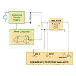
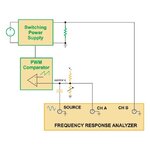
We dont have the money to buy an AP300 Gain/phase analyser to actually measure it in the lab
PRM48BH480T200B00 datasheet:-
https://www.vicorpower.com/documents/datasheets/PRM48BH480T200B00.pdf


