Continue to Site

Welcome to EDAboard.com

Welcome to our site! EDAboard.com is an international Electronics Discussion Forum focused on EDA software, circuits, schematics, books, theory, papers, asic, pld, 8051, DSP, Network, RF, Analog Design, PCB, Service Manuals... and a whole lot more! To participate you need to register. Registration is free. Click here to register now.

What's wrong with my OpAmp?

Status
Not open for further replies.

tony_lth

Advanced Member level 5
Joined
Jul 28, 2010
Messages
2,088
Helped
377
Reputation
756
Reaction score
368
Trophy points
1,363
Location
Beijing
Activity points
12,641
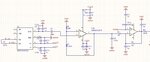
I built a simple OpAmp circuits, using AD8226ARMZ and AD8669ARUZ.
My signal is several Hz, and VREF is 1.2V.
After Diff OpAmp AD8226, I used a 10uF(C7) to isolate DC, I hope pin5 of AD8669 is just small AC signal (about several Hz), but the tested value of pin5 is about 0.6V, and the OpAmp output pin7 is about 3.3V, the up rail of OpAmp.
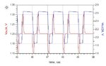
The original design is that C7 at th position of the output of U1B, but that will cause waveform distortion. See attached simualtion result.
So I changed 10uF from output of U1B to input of U1B.
1. What's wrong with it? I designed U1B with AC 750 times amplifies,but obvious DC is very high.
2. Is some ESD diode in AD8669 caused input pins of AD8669 0.6V?
3. I used ADS to simulate my OpAmp circuits, and it works well. Why in real circuit it does not work?
4. Any suggestion about the replacement with AD8669? so that input pins doesn't have 0.6V offset DC voltage?
Thanks.
 

Attachments

  • OpAmp_SCH.JPG
    OpAmp_SCH.JPG
    129 KB · Views: 171
  • OpAmp_Simulate_Result.JPG
    OpAmp_Simulate_Result.JPG
    39.6 KB · Views: 182

Shorting OP output with a capcitor, either 1 nF or 0.22uF, causes instability and in case of doubt self oscillation.

Secondly, there must be a bias resistor after the 10 µF capacitor.
 
hi,
Your circuit shows pin #5, of U1B floating, it needs a path to 0V.
E
 
Hi,

a capacitive load directely connected to a OPAMP output is critical. (at both AD8669 outputs).

What is your intention to do so?

If you want to build a low pass filter, then the resistor is missing.

***
Also the combination of R6 and C14 at inverting OPAMP input is critical. It may lead to oscillations. At least it amplifies the OPAMP´s and V_Ref noise, especially at high frequencies.

Maybe you describe what you want to do...

Klaus
 
OK. I will try and let you know the results.

- - - Updated - - -

Thank you very much.

- - - Updated - - -

HI,
My dsigned circuits are three parts: 1st is diff amp, 2nd is amp with high gain, and 3rd is clamp.
I added the capacitors just want to remove higher freq,
My working signal is only several Hz, but in my module there is RF signal, so I added these capacitors try to remove interference.
I simulated with ADS, and found no issue, so I guess it can work, but never thought there are so much issues.
Thanks. I will try later.
 

Hi,

RF signals.

It is better to suppress RF in the input of an OPAMP that at the output.

With an non inverting OPAMP circuit you may connect a capacitor directely at IN+ to GND. Good design, because the feedback path is not influenced ba the capacitor. But you should calculate a cutoff frequency. Here you need an R in series with the signal.

A capacitor at the inverting input of an OPAMP is critical. For sure it seems to suppress RF coming fromthe signal input. But it also suppresses fast response from the OPAMP feedback path. Therfore the OPAMP circuit has high gain for high frequencies. Additionall this C with the feedback R will generate additional phase shift and this may lead to oscillations.

If your OPAMP is unity gain stable, then a capacitor across the feedback resistor will act like a low pass filter. Suppressing high frequencies. The low pass filter of this circuit is limited by the OPAMPs bandwidth. A slow OPAMP may not be able to actively suppress RF frequencies. That´s why I said it´s better to use the LPF in the input signals.

****
I recommend
* to use a RC LPF at each diff amp input.
* higher gain at the diff amp for lower noise
* decide if you need a second amplifier stage. If you need it, then it should be less gain than the first stage (diff amp).
* Use RF low pass filters to ensure clean signals and to prevent the OPAMP input stages being overdirven by the RF signals

I can´t recognize the third stage as clamp. It is just an inverting AMP with gain of -1 from 0Hz to 80 kHz, then it has increasing gain, until GBW of OPAMP makes the gain decreasing.
There is no defined low pass filter to avoid RF in the whole circuit.


Klaus
 
Thanks. KlausST.
Actually after the 3rd stage output, there is a RC LPF (16.5K+2.2uF). I omitted it here.
Our working freq is several Hz, how to set the port impedance when calculate the RC LPF, as you aforesaid before the diff amp. What I mean is that what value I should set when design the RC value? I think I shouldn't use 50 ohm, so what should I use? because S21 is dependent on this .

- - - Updated - - -

For 3rd stage, I just want to move the bias of negative signal so that ADC can sample it.
 

Hi,

I'd calculate the input filter with the help of the source impedance.
If source is low ohmic, then i'd use the LPF impedance about 10...50 times the source impedance.
For high source impedance i'd choose about the same impedance for the LPF.
..always at cutoff frequency.

Klaus
 
Hi,
I modified as you instructed, remove OpAmp Output shunting capacitors and adding shunting resistors on -In of OpAmp. Many Thanks. Now the last two stages are stable. But the whole circuit is still unstable.
1. For LPF before diff OpAmp, I added shunting capacitors on +In and -In of Diff Amp, NO series resistors before C because no space available on current PCB. It seems work, right?
2. For +In and -In of Diff OpAmp, no resistors to GND, should I added one to stablize the Diff OpAmp?
Thanks.
 

Hi,

Please show us your complete schematic.

And if we should decide if the input circuit is correct, then we need the sensor data.

Klaus
 

Before Diff OpAm is a HSMS2829 (? I can't remember its name) mixer.
It has 4pcs diode as double balance pair. One RF input and one LO input, and two IF output. then mixer output directly link to Diff OpAmp. In the original design, there is no RC filter for LPF, so I followed your instruction that only shunting a 1uF to GND on the traces of the +In and -In. ( Now I am at home, but SCH is in office.) I can only paste SCH on Tuesday.
I guess I have made it clear, right? Could you give some suggestion so that I can try.
 

Hi,

only shunting a 1uF to GND
A single capacitor without (known) series impedance is no good idea.

Klaus
 
Does the +In and -In of Diff OpAmp need resistor to GND?
Or a capacitor across +In and -In for removing interference?
Do you think that's a good idea?
Thanks.
 

Would appreciate a corrected schematic. Which Diff OP are you talking about?

In case you mean AD8226ARMZ, that's an integrated instrumentation amplifier, not an OP.

Obviously any OP input needs a bias current path, might be a resistor to ground in some situations. The same applies to AD8226ARMZ.

A capacitor between In+ and In- of a OP creates a pole in loop gain and may cause instability. But no problem for AD8226ARMZ, there's no feedback path to it's inputs.
 
Sorry, I thought AD8226ARMZ as Diff OpAmp. I mis-understood.
Thanks, FvM and KlausST. Now I am clear about my circuits.
Thanks again.
 

Hi,
Suddenly I found my idea wrong.
Thanks.
 
Last edited:

Status
Not open for further replies.

Similar threads

Part and Inventory Search

Welcome to EDABoard.com

Sponsor

Back
Top