promach
Advanced Member level 4
I have created a series, shunt LC bandstop/notch filter.
https://github.com/promach/frequency_trap/tree/9806e6c293463c1eca3b1b5f0c92ac3e76d14f28


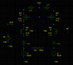
The screenshots above correspond to frequency_trap.net, CMOS_Inverter.net and Gm2.net respectively.
However, when I run "make clean && make" after cloning the project from github, ngspice gave me the following error:
Could anyone advise ?
CMOS_Inverter.net
frequency_trap.net
Gm2.net
https://github.com/promach/frequency_trap/tree/9806e6c293463c1eca3b1b5f0c92ac3e76d14f28


The screenshots above correspond to frequency_trap.net, CMOS_Inverter.net and Gm2.net respectively.
However, when I run "make clean && make" after cloning the project from github, ngspice gave me the following error:
doAnalyses: TRAN: Timestep too small; initial timepoint: trouble with p1-instance m.x1.m4
tran simulation(s) aborted
Could anyone advise ?
CMOS_Inverter.net
Code:
* gnetlist -L ../.. -g spice-noqsi -o CMOS_Inverter.net CMOS_Inverter.sch
* SPICE file generated by spice-noqsi version 20130710
* Send requests or bug reports to [email]jpd@noqsi.com[/email]
.subckt INV1 2 1
M4 1 2 Vdd Vdd P1  l=0.4 w=3         m=25
M1 1 2 Vss Vss N1  l=1.2 w=3         m=25
*
*
.ENDS
frequency_trap.net
Code:
* gnetlist -L ../.. -g spice-noqsi -o frequency_trap.net frequency_trap.sch
* SPICE file generated by spice-noqsi version 20130710
* Send requests or bug reports to [email]jpd@noqsi.com[/email]
Ctest X1.IN Vout 1n
Vd Vdd GND 'SUPPLY'
Vs Vss GND 0V
.GLOBAL Vdd Vss
.INCLUDE CMOS_Inverter.net
.INCLUDE Gm2.net
.INCLUDE active_inductor.net
.PARAM SUPPLY=3.3v
.options TEMP=25
.MODEL n1 NMOS
.MODEL p1 PMOS
Vtest Vtest GND dc 0
+ac 1
CL GND Gm2.IN 0.07pF
XGm2 Gm2.IN Gm2.OUT GM2
X1 X1.IN X1.OUT INV1
V_IP_X1 X1.OUT Gm2.IN DC 0V
V_IP_Gm2 Gm2.OUT X1.IN DC 0V
Rs Vtest Vout 1e99 ac=1e-6
.control
op
ac lin 10000 138 200
write frequency_trap.raw
gnuplot vtest db(vtest)
gnuplot vout db(vout)
*plot Vtest Vout
tran 0.1p 400p
plot Vtest X1.IN X1.OUT
setplot
plot i(v.xgm2.v_ip3) i(v.xgm2.v_ip4) i(v.xgm2.v_ip5) i(v.xgm2.v_ip6)
noise v(Vtest) Vtest lin 100 1 10G
setplot noise1
let noise_figure=db(inoise_spectrum)/2-db(2*sqrt(boltz*290*50))
plot noise_figure
.endc
Gm2.net
Code:
* gnetlist -L ../.. -g spice-noqsi -o Gm2.net Gm2.sch
* SPICE file generated by spice-noqsi version 20130710
* Send requests or bug reports to [email]jpd@noqsi.com[/email]
.subckt GM2 7 3
M4 g3 g3 1 1 P1  l=1u w=3u
M3 3 g3 2 2 P1  l=1u w=3u
M5 3 5 4 Vss N1  l=1u w=3u
M6 g3 7 6 Vss N1  l=1u w=3u
I2 8 Vss 40uA
I1 9 Vss 40uA
Vb 5 Vss 1.8V
Rs 9 8 500k
*
*
V_IP6 6 8 DC 0V
V_IP5 4 9 DC 0V
V_IP4 Vdd 1 DC 0V
V_IP3 Vdd 2 DC 0V
.ENDS