Continue to Site

Welcome to EDAboard.com

Welcome to our site! EDAboard.com is an international Electronics Discussion Forum focused on EDA software, circuits, schematics, books, theory, papers, asic, pld, 8051, DSP, Network, RF, Analog Design, PCB, Service Manuals... and a whole lot more! To participate you need to register. Registration is free. Click here to register now.

VHDL code for the gate circuit

Status
Not open for further replies.

kongruxue

Newbie level 6
Joined
Apr 13, 2012
Messages
14
Helped
0
Reputation
0
Reaction score
0
Trophy points
1,281
Activity points
1,406
Hi, I want to get the gate circuit which shows in the handwrite gate circuit gate_circuit.JPG.
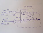
so I wrote the VHDL code below
Code:
LIBRARY ieee;
USE ieee.std_logic_1164.ALL;
USE ieee.numeric_std.ALL;

ENTITY memory_cell IS
PORT
	( I          :IN  std_logic;----input bit
	  W          :IN  std_logic;-----write_enable
	  S          :IN  std_logic;----select_enable
	  clk        :IN  std_logic;
	  q          :OUT std_logic------output bit
	  );
END memory_cell;
ARCHITECTURE structural OF memory_cell IS
SIGNAL J,K,J_g,K_g,Qa,Qb :std_logic;
ATTRIBUTE keep : boolean;
ATTRIBUTE keep OF J_g,K_g,Qa,Qb: SIGNAL IS true;
BEGIN
K <= NOT I AND W AND S;
J <= I AND W AND S;
K_g <= NOT (K AND clk AND Qa);
J_g <= NOT (J AND clk AND Qb);
Qa <= K_g NOR Qb;
Qb <= J_g NOR Qa;

q <= Qa;
END structural;

and I check the RTL Viewer, I get the image
memory_cell.png

but not the same, How do I change the code?
 

All of your assignments are outside of a process so they are implemented in combinatorial logic.

If you want logic to only run on a clock edge, either rising or falling, you should create a clocked process like the following:

Code:
process (clk, rst)
begin
  if (rst = '0') then
    K_g <= '0';
  elsif rising_edge(clk) then
    K_g <= not (K and Qa);
    etc...
  end if;
end process;

You could remove the reset assignment, but somewhere you should initialize the logic so X's don't propagate through the design.
 
  • Like
Reactions: TuAtAu

    TuAtAu

    Points: 2
    Helpful Answer Positive Rating
Gbounce, I think the point here is to CREATE a flip-flop from gates, not just INFER a f-f. With that said, I haven't sat down
and analyzed the two circuits and why they're different (or if they actually are from a functional point of view)
 

Thanks. like Barry said. I want to create a flip-flop from gates. I want the gate circuit exactly the same which shows in the first image. where and how should i change the code to get it? PS .i wrote all codes from gates,so I don't use process.
 

the synthesisor will minimise the gates into something that is functionally identical. you wont be able to stop it. but if you test it it should work identicallty
 

To refer to some comments, the circuit doesn't represent a clock edge sensitive synchronous FF description, and there's no change to infer a FF from it, what ever you do with it.

Second comment, if you want to behave it as level clocked FF, the implementation details can actually matter. We need to ask for the target hardware. If it's FPGA synthesis, there are no real "gates" at all, and all expectations of a particular gate specific behaviour may be void. In return, a FPGA synthesis tool isn't prepared for synthesizing gate structures. An ASIC tool however is.

As TrickyDicky said, the synthesized RTL circuit has apparently the same (statical) logic behaviour. There's a principle option, to assign logic nodes to real logic element by vendor specific synthesis attributes or low level primitives. So you can make the RTL more look like your original circuit. But a FPGA implementation still involves routing delays and possibly glitches of switching logic elements, that aren't present in real gates.
 

Status
Not open for further replies.

Part and Inventory Search

Welcome to EDABoard.com

Sponsor

Back
Top