Continue to Site

Welcome to EDAboard.com

Welcome to our site! EDAboard.com is an international Electronics Discussion Forum focused on EDA software, circuits, schematics, books, theory, papers, asic, pld, 8051, DSP, Network, RF, Analog Design, PCB, Service Manuals... and a whole lot more! To participate you need to register. Registration is free. Click here to register now.

Design of fully differential folded-cascode

Status
Not open for further replies.

joe_sg

Newbie level 1
Joined
Oct 18, 2006
Messages
1
Helped
0
Reputation
0
Reaction score
0
Trophy points
1,281
Activity points
1,296
hi all

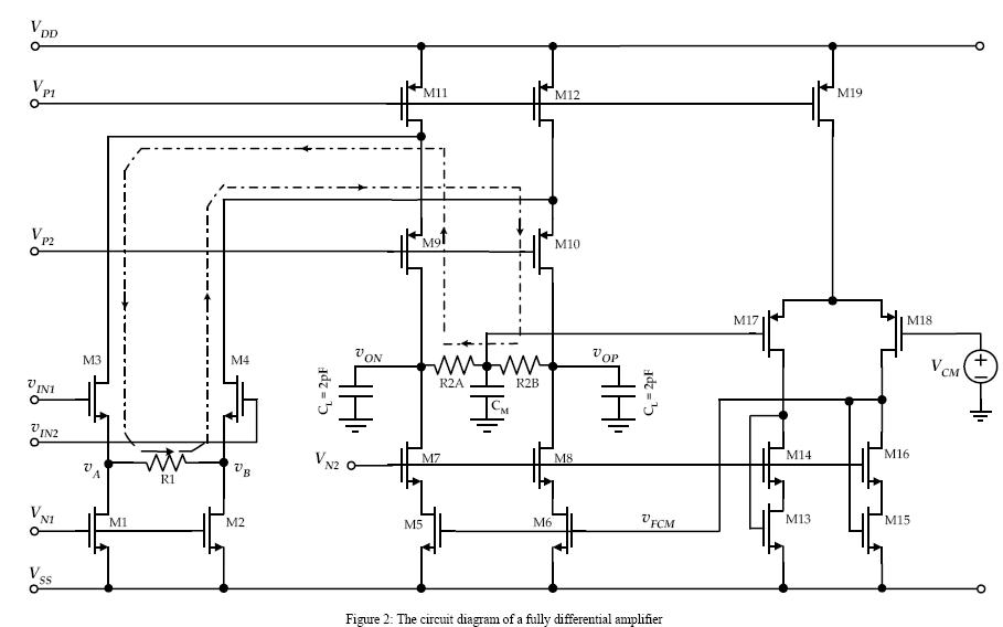
the following circuit is a fully differential folded-cascode op-amp with CMFB.
there is some slight difference with those i have seen on other site.

There is a resistor R1 below the input differential pair, R2A and R2B are used to average the output (Vop and Von). the CMFB circuit compares the average output
with input Vcm and generates feedback Vfcm to control the biasing current
of the output stage.

What is the purpose of R1 , R2A and R2B? how do they affect the differential
gain (Av), unity gain frequency and power? if possible, how to derive the Av
from the circuit? Thanks

https://obrazki.elektroda.pl/84_1161162783.JPG
84_1161162783.JPG
 

R1 for degenration , to a feed back , and make the amplifer more linear for sure this reduce the gain

about Ra , RB to get a sample of ouput voltage common mode , to control the CMFB circuit
i think gain is not affected by these resistors

khouly
 

Hi,

I have a different opinion about the differential gain. The overall gain depends on commom mode resistors and the souce resistor. The gm is reduced by a factor of 1+gm*Rs, where Rs is the source resistor. In the differential mode, the gain will be attenuated if Ra and Rb are not large enough compared with the impedance seen into the cascode devices.

Thanks
 

i think in the design , the impedance at cascode out , very high , and when u design the snse resistor selcet them so that the gain is not affected by them

khouly
 

I think you may remove the Cm cap if you do not want the overall gain drop due to Ra and Rb. Cm cap will provide low impedance at gate of M17, hence your output load will be the parallel effect of cascode impedance and Ra (or Rb).

Perhaps you can place a cap in parallel with Ra (or Rb) to make sure Common mode feedback loop is stable.
 

sengyee88 said:
I think you may remove the Cm cap if you do not want the overall gain drop due to Ra and Rb. Cm cap will provide low impedance at gate of M17, hence your output load will be the parallel effect of cascode impedance and Ra (or Rb).

Perhaps you can place a cap in parallel with Ra (or Rb) to make sure Common mode feedback loop is stable.
hello,
the o/p impedence will include the Ra and Rb wether the cap s there or not cause the point where the cap. is connected is virtual ground in diffrential operation and hence the two resistance will be parallel to the o/p resistance and this cannot be avoided unless u use something like buffer to sense the CM , i think the cap. is added just as a compensation to the CMFB loop
regards
 

I would suggest to use our old friend "half circuit" idea to
analyze the diff. gain. I think the CM capacitor is used
to filter out the common-mode HF disturbance.
 

yschuang said:
Hi,

I have a different opinion about the differential gain. The overall gain depends on commom mode resistors and the souce resistor. The gm is reduced by a factor of 1+gm*Rs, where Rs is the source resistor. In the differential mode, the gain will be attenuated if Ra and Rb are not large enough compared with the impedance seen into the cascode devices.

Thanks
hello,
just a little comment the R1 reduces the gm by factor (1+2gmR1)
regards

Added after 3 minutes:

another comment to uni_student (ur mail aint working ,it gives failur to deliver so hope u see it here):::::::::::
since the two resistors are conected to the o/p of the differentail amp. they see differential o/p (i.e. they are connected to Vop and Von which are diffrentail) so by superposition Vx=Vop*R2a/(R2a+R2b)+Von*R2b/(R2a+R2b)
given that R2a=R2b and Vop=-Von then Vx=0 i.e. virtual ground

about R1 it is degeneration resistance(as was mentioned in a previous post) it is used to increase the linearity of the OTA but it has a side effect of decreasing the gain as it decrease the equivelant Gm of the OTA >>>>Gm=gm/(1+2gmR1)
regards
ahmed safwat
 

Status
Not open for further replies.

Similar threads

Part and Inventory Search

Welcome to EDABoard.com

Sponsor

Back
Top