Welcome to our site! EDAboard.com is an international Electronics Discussion Forum focused on EDA software, circuits, schematics, books, theory, papers, asic, pld, 8051, DSP, Network, RF, Analog Design, PCB, Service Manuals... and a whole lot more! To participate you need to register. Registration is free. Click here to register now.
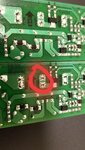
Much of what you see in PCB layouts comes from personal styles, but in this particular case if there was any science behind perhaps the designer believed that by adding vias around the PAD that undergoes mechanical stress on the connector at the opposite side, it could somehow 'sew' the copper sheet more strongly on the board's surface.
Faston terminals, as supposed; this type of connection should not be used in phenolite boards because after a certain amount of handling break the weld. and detach the copper track right below.
It isn't a pad, its solder resist mask. It would normally be included in the footprint of the blade connector but it should be easy enough to create if you need it for something else. It does increase the current capacity but it is mostly to add rigidity to the terminal which obviously will need some pressure to connect or disconnect a cable to.
This site uses cookies to help personalise content, tailor your experience and to keep you logged in if you register.
By continuing to use this site, you are consenting to our use of cookies.