Continue to Site

Welcome to EDAboard.com

Welcome to our site! EDAboard.com is an international Electronics Discussion Forum focused on EDA software, circuits, schematics, books, theory, papers, asic, pld, 8051, DSP, Network, RF, Analog Design, PCB, Service Manuals... and a whole lot more! To participate you need to register. Registration is free. Click here to register now.

Require a Desgin of A MOSFET based Switch , for study purpose .

Status
Not open for further replies.

thannara123

Advanced Member level 5
Joined
Jan 7, 2010
Messages
1,576
Helped
122
Reputation
244
Reaction score
114
Trophy points
1,353
Location
India
Activity points
10,343
I am stauding the MOSFET caharcterstics ,
May I get a Desgin for a MOSFET based Switch for ON and OFF .
with least resistance and maximum current .
Where I start ?
I can choose any MOSFET so please help me?
 

Hi,

MOSFETS have the internal body diode, that may not be wanted with switches.
Other FET don't have the diode.

Did you do an internet search for "FETs as switch" circuit?
Many articles with explanations and calculations are available. Study them.
Did you read any MOSFET datasheet? Resistance and current is given in every datasheet.

Generally you may use any (MOS)FET .... but nobody can tell you which one to choose as long as you don't give any specification.

Klaus
 
"MOSFET based switch" might refer to a solid state relays circuit rather than a bare MOSFET. In any case, you should specify voltage and current rating, in case of a relays circuit also control voltage, isolation and speed rating.
 
Consider this only for learning purpose .
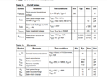
I am Choosing N Channel MOSFET 90NF03L https://www.st.com/resource/en/datasheet/stp90nf03l.pdf
1.PNG2.PNG

As per datasheet ,

Countinues Current @ 100degree The Current Id is 65 A
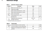
Maximum VDS 30 volt

My load has 20 watt (LED Bulb) so the aproximate Current 1.7 Amp and VDD as 12 Volt .
So I takes as follows

Vdd = 12 volt
Id = 2Amp

Switch has two Position ie ,Cutoff and Saturation

So Cutoff = Vgs<Vth ---- = 0 volt ----> MOSFET OFF.

At switch Close Position ---> saturation

Vds>Vgs-Vth

So I takes Vgs as 10Volt .


is it correct way .or pleas lead me correct way
What is the other considrations ?
is require surge protection circuits ,cappacitance ,Gate resistance ?
 

Hi,

At first please clarify the expected function:

In your first post you wrote "MOSFET based Switch for ON and OFF".
Thus my first idea was a circuit like a bilateral analog switch fir signals...
But now it rather seems like a "low side power switch"

To your specifications:
A Mosfet needs to withstand:
* the maximum applied voltage V_DS --> in your case the supply voltage (plus some headroom)
* the maximum drain current --> in your case the load current (plus some headroom)
* the temperature = maximum ambient temperature + temperature rise caused by I_drain_RMS ^2 × R_ds_on

And yes, V_gs should be close to zero to switch OFF the Mosfet
And should be much higher thanV_gs_th but lower than V_gs_max to switch ON the Mosfet.

Mind: any inductance will cause voltage spikes during switch/OFF. You need to take care that this is less than V_DS_max .... in any case and even for nanoseconds.

Klaus

Then
is correct My aproximation?
 

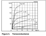
Don't look at Vgs(th) because that is the gate-source voltage when the Mosfet is almost turned off and it is barely turned on. Since you want a switch then you should look at the leakage current when the Vgs is 0V and look at the Vgs voltage at a certain maximum on resistance. The Mosfet you selected is fully turned on when Vgs is 10V and it is turned on pretty well when Vgs is 5V.

For your fairly small current of only 1.6A then using that Mosfet rated at 90A is probably throwing away a lot of money. Use a smaller, less expensive Mosfet which will still have a rating much higher than you need.
 
Switch has two Position ie ,Cutoff and Saturation

So Cutoff = Vgs<Vth ---- = 0 volt ----> MOSFET OFF.

At switch Close Position ---> saturation

Vds>Vgs-Vth

So I takes Vgs as 10Volt .
Vgs = 10V is good (low Rdson, low switch voltage drop), but the "on" operation point is not saturation, it's ohmic mode.
 

If Vgs is 11volt and Vds is 10 volt it saying that Ohmic region .
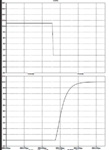
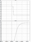
Triode region.PNGsaturationregion.PNGCapture.PNG

As per the ohmic and saturation region the plots shows no diffrents why so .

What is the wrong with me ?
 

And Comonly what type of protections are required for a MOSFET.
 

As per the ohmic and saturation region the plots shows no diffrents why so .

What is the wrong with me?
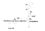
V1 is the supply voltage, not Vds. Vds in on-state is in the mV range, both for V1 =10 and V1=12V.
 
V1 is the supply voltage, not Vds. Vds in on-state is in the mV range, both for V1 =10 and V1=12V.

confused a little :-?
Mesuare the Vds when it ON it gives 12mv and 10.5mv for V1 =12v and V1 = 10 respectively .
 

Measure the Vds when it ON it gives 12mv and 10.5mv for V1 =12v and V1 = 10 respectively.
Should be considered ohmic range, isn't it.

The supply voltage is dropped at R1.
 

e.PNG
How can i attain in ohmic / Triode region ?
As per the data sheet The Vds should be in the range of 2.5volt for the ohmic region.
and Vgs is 5volt .

In the above circuit ,
V2 is the Vgs volt at the ON time isnt it ? it have 11 volt ..
And is the VDD volt will be the Vds volt (which will be appere the Vds after load drop) ?

I want a desgin as follows ?may get with calculation

i need control a bulb 12 volt ,2 Amp. which is controlled by the Vgs of the above MOSFET .
 

The graphs on a datasheet are usually for a Mosfet or transistor with "typical" spec's. Yours might have different minimum or maximum spec's. The text in a datasheet shows minimum and maximum spec's.
You will need to design a circuit with an adjustment for matching the spec's of the Mosfet you use. Sometimes adding negative feedback can reduce the range of spec's.

You said that you want to "control" a 12V/2A bulb. To turn it on and off? The Mosfet datasheet says the Mosfet is off when Vgs is zero and it is turned on well when Vgs is 10V.
 

You said that you want to "control" a 12V/2A bulb. To turn it on and off? The Mosfet datasheet says the Mosfet is off when Vgs is zero and it is turned on well when Vgs is 10V.[/QUOTE said:
Thanks ,
But then Is the MOSFET works on cutoff and Ohmic region ?
or cutoff and stauration region?
 

You are still missing a basic understanding of MOSFET operation.

To get a better idea, you can use the post #9 simulation circuit and perform a dc sweep as shown below. Determine for which Id and Vds range the transistor is in cutoff, saturation and ohmic mode. You'll find that a transistor switch is only temporarily in saturation, you want to avoid this operation due to high power dissipation.

dcsweep.PNG
 
You are confused about Mosfet operation because you are using English terms for an ordinary transistor.
An ordinary transistor is linear when it is partially turned on. It is saturated when it is turned so that it has a low Vce.

But a Mosfet is said to be "saturated" when it is partially turned on and it is "linear" or "ohmic" when it is turned on so that it has a low Vds.
Hai sir i don't have confusion as you said . I know ohmic or linear or triode region is the low resistance mode of the MOSFET operation. Where the condition also known Vds <Vgs-Vth.

I am confused with how attain the ohmic region.and it's calculations
I have to test the simulation as per FvM.
 

The spec's for every Mosfet show its maximum on-resistance when Vgs is 10V. Some Mosfets are called "logic level" and they show the maximum on resistance when Vgs is 4.5V or 5V. There is nothing to calculate unless you test the on resistance of each Mosfet you are using (each one is different even if they have the same part number). You might find (not calculate) a Mosfet that turns on well with a lower Vgs. Like a transistor, a Mosfet has a range of spec's. Some are minimum and some are maximum.

A simulation uses a device with a "typical" on resistance and a "typical" Vgs. But the spec's for the Mosfet you use might be different from a "typical" Mosfet.
 
Status
Not open for further replies.

Similar threads

Part and Inventory Search

Welcome to EDABoard.com

Sponsor

Back
Top