Continue to Site

Welcome to EDAboard.com

Welcome to our site! EDAboard.com is an international Electronics Discussion Forum focused on EDA software, circuits, schematics, books, theory, papers, asic, pld, 8051, DSP, Network, RF, Analog Design, PCB, Service Manuals... and a whole lot more! To participate you need to register. Registration is free. Click here to register now.

current-mode boost converter UC3845

Status
Not open for further replies.

yoosefheidari

Member level 5
Joined
Aug 31, 2013
Messages
91
Helped
0
Reputation
0
Reaction score
1
Trophy points
1,288
Activity points
2,051
hi everyone
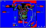
idesign this circuit to bosst voltage from 15v to 36v
in no load condition everything is ok and output voltage is 36v but when i put 7 ohm load in output voltage drop to about 15.5 volt and current about 2.5 amp.
where is problem?why voltage drop from 36 volt to 15.5 under load?
i add 56k resistor beetwen pin3 & pin4 for slope compensation.
BOOST.jpg
uc3845.jpg
 

Hi,

Often made mistake: wrong (saturating) inductance.
--> So please post a link to the inductor's datasheet.

Next most often mistake: Unsuitable PCB layout.
--> Please post your PCB layout, where we can see the complete signal routing, especially the solid GND plane.

Btw: There are many similar threads here. (Different ICs). Read through them.
In more than 90% you see one if the above mistakes.

Klaus

my circuit power is about 400 watt which mean 15v/25A input and 36v/12A output so i use 2 hand wind 55uh inductor in series and 2 parallel diode.pcb is double layer
inductor uses er28 core(pc40 material)31 turn and 2.5mm gap.i measure inductance by accurate LCR meter and was 55uh
under 6 ohm load (40 watt due to voltage drop) board make a pretty load noise like old CRT tv

1.jpg 2.jpg

photo_2019-11-02_11-01-55.jpg
 

Hi,

Now we have:
* self made inductance.
We simply can't verify. There is a good chance that they are not suitable.
Besides the inductance value... the saturation behaviour is very important.

* No GND plane.
A couple of big copper areas is no "low impedance GND plane".
I assume there is no way around a redesign.

* big resistors:
Most probably "wire wound" which means "high series inductance".
If they are in the switching path (what we can't verfy, then they are completely unsuitable.

All informations for a reliably working SMPS are given in the datasheet and application notes provided by the IC manufacturer.
Read them and design the SMPS according this informations ... and it will work.

Btw: the part names in the schematic don't match to the PCB part names. It's a huge ammount of effort for us to find out which part is which part. I don't want to spend that much time...

Klaus
i change the big resistor and put a film resistor but any change happened
here part names match to the pcb parts; is there any problem?
is feedback correct?

BOOST.jpg

1.jpg 2.jpg
 

Hi,

What´s the benefit of using 4 diodes in parallel?
Did you do calculations?

In best case (Equal current distribution) you get a 18% improvement in power dissipation (which should not be much benefit)...but get the drawback of 4 times the capacitance (huge capacitance!)
But in reality I expect that the hottest diode will carry the most current and get even hotter. Maybe one diode carries 80% of the total current and the other diodes in total 20%.

--> Read application notes about paralleling diodes.


Klaus

current can goes up to 35 amp so i use a 40 amp diode with another for overcurrent situation.
my big question is about voltage feedback.is that correct?
 

Hi,

Feedback:

I don´t think it´s correct ... but I can´t fully verify because you don´t give the value of "POT".

I didn´t go through the complete datasheet...but
* I don´t understand why you use R6 at all. What´s your idea behind it?
* the value of R5 seems to me a bit too low. Other values in the datasheet are 150k as an example.

The formula of page13, upper circuit should be corrected to: V_O = 2.5 x (R2 / R1 +1)
In your case
* R2 = 56k
* R1 = 10k + pot_value

Do some caclulations on your own.

BTW: The part seems to be obsolete. I recommend to choose a more modern one. Maybe with synchronous rectifier.

Klaus
 
Have you calculated the Bmax in the chokes for 25A ... ? if it goes above 0.3 Tesla you are in trouble,

Can your power source supply all the amps you need? or does it sag in volts due to connecting wires or internal current limit..?

- - - Updated - - -

B^2 = Uo. L . I^2 / ( Ae . Lg ) Uo = 1.256 E-6, Ae = core centre leg area in m^2, Lg = gap in centre leg + gap in outer leg in metres. 1mm = 0.001 m.

- - - Updated - - -

increase C4 from 100pF to 1nF right on the pins of the controller ...

- - - Updated - - -

put 1.0uF ( or bigger ) film/foil cap 100V across the ends of the current sense resistors - this will reduce the inductive effect of these R's ( which is most of your problem )

- - - Updated - - -

your chokes are in series - it would be far better to design them to be in parallel - 12.5A each ....

- - - Updated - - -

You need some large film/foil 100V caps right after the main diodes to catch the current as it commutates to the output electro - the electro on its own is not enough and you will get very high overvolt spikes when the fet turns off - put at least 10uF 100F film foil from the output diodes to local power ground

- - - Updated - - -

also - do your self a favour - and set the gate resistor to 33 ohm for starters - this will reduce RFI and let you get the ckt going a little bit so you can fix the other issues listed above ....
 
Simulation of simple boost converter with your spec supply and output, showing expected waveforms.

boost conv clk-driv 15VDC supply 55uH 8kHz 36V to 3 ohm load.png

Notice the peak Ampere levels needed to produce 12A at 36V output. Obviously it's much more than 25A from a 15V supply.
Consider interleaving two or more boost converters.
 

total L = 110uH I think - from reading OP's posts, there are two chokes in series ... that will reduce the peak current a bit - but yes - unless the OP's power source can supply the necessary pk currents - testing will be difficult / impossible ...

- - - Updated - - -

Oh - why did you simulate 8kHz..? is that what the RC on the IC gave? 50-70 kHz would be a better operating point I'm thinking - lower peak input current again ...

- - - Updated - - -

I see that 1nF, 22k on that chip gives about 60kHz ...

- - - Updated - - -

the 3845 is 50% PWM drive max - so that limits the o/p to ~ 2x the Vin, so 15 to 30DC out at best ....
 

why did you simulate 8kHz..?
...
I see that 1nF, 22k on that chip gives about 60kHz ...

I adjusted for a slower frequency, in order to bring out the appearance of ramping waveforms, and to help emphasize the massive Ampere levels.

60 kHz operation may very well be correct, however coil current is smoothed until it's like a DC waveform about 35 A, and the other waveforms resemble pulsed DC square waves. Output V takes many cycles to stabilize. The boost converter action is not as obvious.
 

The noise you're hearing is inductor saturation.

- - - Updated - - -

Your major issue seems to be your duty cycle. Your duty cycle may be saturating. uc3845 has maximum of 46% or thereabout duty cycle

- - - Updated - - -

Without modeling loss elements, your duty cycle is above 50% already.
 

For ER28 with 2.5mm centre pole gap ( or 1.25mm right thru ) for 55uH and 25Apk the Bpk = 459mT which is too high, the gap needs to increase by 459/300 = 53% on the 2.5mm i.e. total gap needs to be 3.825mm to keep you just this side of saturation for 25A ( the L will drop by the same factor: 300/459 to 36uH, x2 for two chokes in series)

the current ripple at 50% duty cycle, 15Vin & 70kHz say will be 1.48 amps pk-pk so nothing to worry about - but the duty cycle needed for Vin = 15V, Vo = 36V = 60%

as Vo/Vin = 1/(1-D) in CCM for a boost, 60% gives 2.5x 15 = 37.5 to allow for diode drop & other losses ...

So you will need another IC in a DIP8 package ( there are plenty )

good luck ...

- - - Updated - - -

p.s. you still need a power supply or battery and cables that can reliably supply 25A ( and a bit more ) at a solid 15VDC - if the power supply sags your full power testing will be very difficult indeed ...
 

always do a representative simulation before doing a power supply. LTspice is free and the LT124X series is the same almost as UC384X.

- - - Updated - - -

here is your simulation....in ltspice which is free on the web....you can run this and get your head into it...by the way, you will need a current sense transformer for the uc384x range.,.....i gave it to you in the sim

- - - Updated - - -

chnage the .txt to .asc, then open it, then hit running man icon....and you see it.

Your problems coudl also be due to your not using a current sense transformer...the sense voltage on uc384x is 1v...very high for your high current

- - - Updated - - -

If you are trying to design an smps without doing a representative simulation, you are like a climber who attempts everest without taking a food supply....best of luck!

- - - Updated - - -

Also, please use my free SMPS course, which is found in this website somewhere
https://massey276.wixsite.com/electronicsdegree
 

Attachments

  • UC384x.txt
    5.6 KB · Views: 74
Last edited by a moderator:
thank you all guys
after those problems i decide to use LT3782 dual phase interleaved boost controller and some changes in specifications like Vin is same 15 Vout is 30volts input current is 14amps.
after design pcb in altium and build the circuit there is a little problem.
to set current limit at 14 amps(two 7amps) i use two 0.008ohm resistor but total output current limited to 2.3 amps!i think problem is noises on sense path because when i connetc +sense and -sense pins to ground there is no problem and output current is 7 amps at 30 volts.
this is input current when senses pins are grounded.average currnet is 14 amp and there is frequently 25amps picks.i thin these pick are cause of current sense resistor limitation problem.am i right?
photo_2019-11-12_13-04-20.jpg
how can i remove these picks?without current sense resistor somtimes right mosfet burn immediately.
input voltage is from a 15V/30A half bridge switching supply and when i connect it to my board; that supply make a bad noise(probably output inductor)
https://www.analog.com/media/en/technical-documentation/data-sheets/3782fg.pdf

2565.jpg
red.jpg
photo_2019-11-11_21-23-24.jpg
 

Attachments

  • abi.jpg
    abi.jpg
    153.1 KB · Views: 429
Last edited:

did you kelvin connect the sense resistor?
Did you put a gate series resistor to damp the fet switch on?
 

Hi,

I have to repeat what's written in post#2 and post#4 about GND plane.

Klaus
 

did you kelvin connect the sense resistor?
Did you put a gate series resistor to damp the fet switch on?
yes i use kevin sensing method but path length is about 4 centimeter. is that very bad?
i use a ir4427 driver between lt3782 and mosfet to protect lt3782 because it is very sensitive.i put a 4/7 ohm resistor between ir4427 and mosfet's gate.
without current sense resistor circuit wors but sometimes the right mosfet burn by unknown reason.

- - - Updated - - -

Hi,

I have to repeat what's written in post#2 and post#4 about GND plane.

Klaus

can you please give me a good source about ground plane in pcb design to read?
 

Status
Not open for further replies.

Similar threads

Part and Inventory Search

Welcome to EDABoard.com

Sponsor

Back
Top