Continue to Site

Welcome to EDAboard.com

Welcome to our site! EDAboard.com is an international Electronics Discussion Forum focused on EDA software, circuits, schematics, books, theory, papers, asic, pld, 8051, DSP, Network, RF, Analog Design, PCB, Service Manuals... and a whole lot more! To participate you need to register. Registration is free. Click here to register now.

Parasatic effect of the dummy transistor

Status
Not open for further replies.

Junus2012

Advanced Member level 5
Joined
Jan 9, 2012
Messages
1,552
Helped
47
Reputation
98
Reaction score
53
Trophy points
1,328
Location
Italy
Activity points
15,235
Dear friends

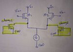
I am matching my circuit layout with dummies connected as shown below. I am connecting the dummy transistor as usual instance in the schematic circuit so the LVS will not complain when he compare.

I see this connection from one website but I am wondering that this dummy connection would add parasatic capacitance to the node where it is connected.

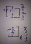
Is it possible to avoide this connection with other type, for example using PMOS with gate, source and drain tied together and connected to Vdd, for the NMOS gate, source and drain tie together and connected to gnd

Thank you in advance
New Doc 55.jpg
 

The dummies are for lithographic matching at lower layers
(N+/P+, active, poly, contact) and they are unlikely to be
helpful as "baggage" on live circuit nodes. I would tie off
the active terminals to the body tap.
 
Dear freebird

Yes indeed i am using the dummies for the purpose of lithographic matching. by putting dummy transistor it is already has the N+ or P+, active, poly, contact just like you mentioned.

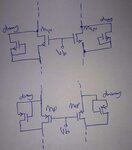
However, gorgive me please if I didn't get exactly your suggestion of connecting the dummy transistor, do you mean I connect the drain, gate and the source to the transistor body (bulk terminal), if so then it means for PMOS I will connect them to VDD as I mostly use to connect the PMOS bulk to the VDD (for some transistors I tie it to the source) and for the NMOS to the ground, as shown below

by this connection the transistor is not connected to any circuit node and thus has no parasitics contribution

please correct me if I am wrong amd thank you again

New Doc 56.jpg
 

You put dummies either at the two ends of a contiguous OD area to match/avoid WPE or environment contributions on matching of devices inside the active array. In other words, create equal conditions for all devices that need to match. Thus, at least one of the dummies will have to share a node with the active devices. This common node can be vdd or gnd but not always. If you can, connect S,D, G together (bulk is usually common for the active and dummy devices). This is not always possible, in which case one of the terminals of the dummy will be connected separately from the rest. In this case that dummy will contribute to parasitic caps in the node. That's unavoidable. You just have to think how to connect dummies, where to place them etc, based on the way you lay out your active devices.
 
Last edited:
Dear Suta,

Nice to hear from you and thank you for your explanation,

I would say regarding of what you have explained that the if VDD or GND is a common node like the down NMOS array or the upper PMOS array then connecting the dummy terminals to the VDD or GND will have no effect on the mirror node and no parasatics.

Howver, if our matched array is in the middle then we must share the node with the dummy and by this way as you said it is not possible to avoid the the parasatics. for the NMOS I will connect all te terminals together then to the node and to the substrate.

I think it is better to give you graph, soon I will upload it

thank you

- - - Updated - - -

here is the picture

New Doc 57.jpg

Also Suta I would like to ask you please about your method of defining the dummies in cadence, for me I am using such a trick by putting these devices in the schematic so the LVS will have no problem. However I believe there is better or shorcut method to do it. is it possible to make it wih lvsIgnore ? or there is may be a layer in the layout tool when I cover it with that layer it will be igonered

thank you once again
 

It will be much better if the dummies for the bottom NMOS transistors M7/8 are connected to gnd with all terminals shorted (of course, if possible). They will be out of the picture in this case. The way you've shown them connected is not correct because you short the drain of M7/8 to gnd - but probably it is just a drawing error.


Our layouters here always put the dummy transistors in the schematic and no extra tricks to be ignored by LVS. I think that's the cleanest approach.

Dear Suta,

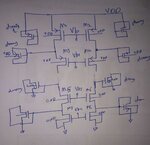
I have corrected the dummy transistor connections as shown below, kindly could you tell me please that it is now ok

thank you

New Doc 58.jpg
 

Looks ok. It will be even better if you can connect the drains of dummy7/8 to gnd too, as well as, the drains of dummy1/2 to vdd. Also, is it possible to connect the drains of dummy5/6 to the sources of M5/6 instead and dummy3/4 to the sources of M3/4?
 
Dear Suta,

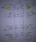
I modified the circuit according to you kind last comment,

You asked me "Also, is it possible to connect the drains of dummy5/6 to the sources of M5/6 instead and dummy3/4 to the sources of M3/4?", Actually I don't know a reason which doesn't allow, is it related to the used technology ?

New Doc 59.jpg

by the way, according to my last plot (based on you explanation), the dummy transistors do not share any node with the circuit (except the VDD and the GND) and therefore I think they will add parasatic effects


I am looking forward for your confirmation

Thank you onc e again
 

Dear Suta,

I think for the circuit I shown it is possible to connect the drain to the ground for NMOS and to the VDD for the PMOS. However, for matching differential pair this will not be possible if we need to include the dummy in the same structure of the matched bar transistors. Unless if we put the dummies just beside the matched array then it will be possible but the dummy will lose the importance and the purpose of the placement
 

I have the feeling that your dummies are not in the same OD as the transistors they are dummies for. Otherwise how can you connect the dummies for the cascode devices with all terminals to gnd or vdd? If those are dummies for the cascodes then they have to have one node common with the cascodes (at least one dummy in case you use more than one in the array).

The dummies for the diff pair are bes connected to the tail node since it is virtual ground with the consequence that they might worsen the CMRR at higher frequencies.
 
Dear Suta,

Thank you for your help

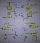
These are my final scheme for connecting the dummy transistors according to your kind explanation

New Doc 58.jpg

New Doc 60 1.jpg
 

Let me understand something. Are you putting dummies in the schematic before you place them in the layout or you first put dummies in the layout according to what is possible and necessary and then reflect that in the schematic?
 
Dear Suta,

during my layout when I do the matched array I put my dummy then I go to schematic to see if it has a problem with some simulation and also to pass the LVS check, if every thing ok I continue in my layout
 

I understand now. So, how are your simulations with the latest dummy placement?
 
Dear Suta,

the simualation is giving me a very good results specially when you suggested me to onnect the dummy to the common source terminal of the differential amplifier and it is giving better AC result comparing to the first state when I connected to the drain. Almost nigligable loading effect and nigligable change in the AC simulation. I will continue using your approach in the last two pictures for the rest of my layout.

I am very grateful for your support
 

Status
Not open for further replies.

Part and Inventory Search

Welcome to EDABoard.com

Sponsor

Back
Top