AjayKhedekar
Newbie level 3
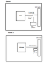
I am designing Main board using Altera FPGA. In circuit I need external differential clock. On main board I have introduce one clock generator circuit also have provision to take clock from external daughter board. Clock frequency range is 10-200 MHz. There are two possibilities but at time one source is selected
1) On board clock generation to FPGA
2) From external board to FPGA
In this can I use male berg pin for clock source selection between on board circuit or external board? If I use Berg pin does it affect on clock signal in any way?
I can use clock multiplexing IC, still it will increase lot of hardware as I have 4 clock input signals. One more option to place clock generation circuit near possible to header and directly shorting trace without any jumper?
Does Berg pin harm in this condition? If yes what are the different effect on clock signal?
If I directly merge the both signals what are the different effect of same.
As I have seen lot of board on which berg pin jumper is used for selection clock source but it have smaller frequency range like 5 MHz. One of the reference from Microchip is here. https://www.microchip.com/webdoc/stk500/stk500.clock.settings.html
