msdarvishi
Full Member level 4
Dear all,
I am using Vivado 2017.3 and a Sundance board including a XC7K410T FFG900 Xilinx FPGA.
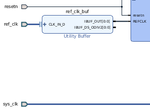
I have a block design that I have instantiated two clock signals in it, ref_clk that is connected to the PCIe reference clock pin of a AXI Memory Mapped to PCI Express module. Both clock signals are defined by defined by Tcl command for interface clock creation, and the sys_clk that is connected to the MIG 7 Series as shown below.

My Tcl commands for clock generations are as follows:
and here are the constraints that I have written in an XDC file for both clock siugnals:
While Placement design the process fails and I receive the following Placement Error [Place 30-172]
I have tries lots of scenarios and methods to solve this problem but it still does exist. I am really confused! Can anyone help me to solve this issue, please?
Kind helps are in advance appreciated.
Bests,
I am using Vivado 2017.3 and a Sundance board including a XC7K410T FFG900 Xilinx FPGA.
I have a block design that I have instantiated two clock signals in it, ref_clk that is connected to the PCIe reference clock pin of a AXI Memory Mapped to PCI Express module. Both clock signals are defined by defined by Tcl command for interface clock creation, and the sys_clk that is connected to the MIG 7 Series as shown below.

My Tcl commands for clock generations are as follows:
Code:
# ---------- SYS_CLK for MIG 7 Series DDR3 SDRAM

create_bd_intf_port -mode Slave -vlnv xilinx.com:interface:diff_clock_rtl:1.0 sys_clk
connect_bd_intf_net [get_bd_intf_pins mig_7series_1/SYS_CLK] [get_bd_intf_ports sys_clk]


# ------------ ref_clk for PCIe module
create_bd_intf_port -mode Slave -vlnv xilinx.com:interface:diff_clock_rtl:1.0 ref_clk
connect_bd_net [get_bd_pins ref_clk_buf/IBUF_OUT] [get_bd_pins axi_pcie_0/REFCLK]
and here are the constraints that I have written in an XDC file for both clock siugnals:
Code:
# --- ref_clk (for PCIe)
set_property PACKAGE_PIN U8 [get_ports {ref_clk_clk_p[0]}]
set_property PACKAGE_PIN U7 [get_ports {ref_clk_clk_n[0]}]


# --- SYS_CLK
set_property PACKAGE_PIN K28 [get_ports {sys_clk_clk_p}]
set_property PACKAGE_PIN K29 [get_ports {sys_clk_clk_n}]
While Placement design the process fails and I receive the following Placement Error [Place 30-172]
Code:
[Place 30-172] Sub-optimal placement for a clock-capable IO pin and PLL pair. If this sub optimal condition is acceptable for this design, you may use the CLOCK_DEDICATED_ROUTE constraint in the .xdc file to demote this message to a WARNING. However, the use of this override is highly discouraged. These examples can be used directly in the .xdc file to override this clock rule.
	< set_property CLOCK_DEDICATED_ROUTE ANY_CMT_COLUMN [get_nets ublaze_i/mig_7series_1/u_ublaze_mig_7series_1_1_mig/u_ddr3_clk_ibuf/sys_clk_ibufg] >

	ublaze_i/mig_7series_1/u_ublaze_mig_7series_1_1_mig/u_ddr3_clk_ibuf/diff_input_clk.u_ibufg_sys_clk (IBUFDS.O) is locked to IOB_X0Y174
	 ublaze_i/mig_7series_1/u_ublaze_mig_7series_1_1_mig/u_ddr3_infrastructure/plle2_i (PLLE2_ADV.CLKIN1) is locked to PLLE2_ADV_X1Y1

	The above error could possibly be related to other connected instances. Following is a list of
	all the related clock rules and their respective instances.

	Clock Rule: rule_gclkio_bufg
	Status: PASS
	Rule Description: An IOB driving a BUFG must use a CCIO in the same half side (top/bottom) of chip
	as the BUFG
	 ublaze_i/mig_7series_1/u_ublaze_mig_7series_1_1_mig/u_ddr3_clk_ibuf/diff_input_clk.u_ibufg_sys_clk (IBUFDS.O) is locked to IOB_X0Y174
	 ublaze_i/mig_7series_1/u_ublaze_mig_7series_1_1_mig/u_iodelay_ctrl/clk_ref_200.u_bufg_clk_ref (BUFG.I) is provisionally placed by clockplacer on BUFGCTRL_X0Y7

	Clock Rule: rule_gclkio_mmcm_cdr_bb
	Status: PASS
	Rule Description: An IOB driving an MMCM must both be in the same column clock regions if CLOCK_DEDICATED_ROUTE=BACKBONE
	is set
	 ublaze_i/mig_7series_1/u_ublaze_mig_7series_1_1_mig/u_ddr3_clk_ibuf/diff_input_clk.u_ibufg_sys_clk (IBUFDS.O) is locked to IOB_X0Y174
	 ublaze_i/mig_7series_1/u_ublaze_mig_7series_1_1_mig/u_iodelay_ctrl/clk_ref_mmcm_gen.mmcm_i (MMCME2_ADV.CLKIN1) is provisionally placed by clockplacer on MMCME2_ADV_X0Y6

	Clock Rule: rule_mmcm_bufg
	Status: PASS
	Rule Description: An MMCM driving a BUFG must be placed on the same half side (top/bottom) of the device
	 ublaze_i/mig_7series_1/u_ublaze_mig_7series_1_1_mig/u_iodelay_ctrl/clk_ref_mmcm_gen.mmcm_i (MMCME2_ADV.CLKOUT1) is provisionally placed by clockplacer on MMCME2_ADV_X0Y6
	 ublaze_i/mig_7series_1/u_ublaze_mig_7series_1_1_mig/u_iodelay_ctrl/clk_ref_300_400_en.clk_ref_400.u_bufg_clk_ref_400 (BUFG.I) is provisionally placed by clockplacer on BUFGCTRL_X0Y16

	Clock Rule: rule_mmcm_mmcm
	Status: PASS
	Rule Description: An MMCM driving an MMCM must be in the same CMT column, and they are adjacent to
	each other (vertically), if the  CLOCK_DEDICATED_ROUTE=BACKBONE constraint is NOT set
	 ublaze_i/mig_7series_1/u_ublaze_mig_7series_1_1_mig/u_iodelay_ctrl/clk_ref_mmcm_gen.mmcm_i (MMCME2_ADV.CLKFBOUT) is provisionally placed by clockplacer on MMCME2_ADV_X0Y6
	 ublaze_i/mig_7series_1/u_ublaze_mig_7series_1_1_mig/u_iodelay_ctrl/clk_ref_mmcm_gen.mmcm_i (MMCME2_ADV.CLKFBIN) is provisionally placed by clockplacer on MMCME2_ADV_X0Y6

	Clock Rule: rule_pll_bufhce
	Status: PASS
	Rule Description: A PLL driving a BUFH must both be in the same horizontal row (clockregion-wise)
	 ublaze_i/mig_7series_1/u_ublaze_mig_7series_1_1_mig/u_ddr3_infrastructure/plle2_i (PLLE2_ADV.CLKOUT3) is locked to PLLE2_ADV_X1Y1
	 ublaze_i/mig_7series_1/u_ublaze_mig_7series_1_1_mig/u_ddr3_infrastructure/u_bufh_pll_clk3 (BUFH.I) is provisionally placed by clockplacer on BUFHCE_X1Y12

	Clock Rule: rule_bufh_bufr_ramb
	Status: PASS
	Rule Description: Reginal buffers in the same clock region must drive a total number of brams less
	than the capacity of the region
	 ublaze_i/mig_7series_1/u_ublaze_mig_7series_1_1_mig/u_ddr3_infrastructure/u_bufh_pll_clk3 (BUFH.O) is provisionally placed by clockplacer on BUFHCE_X1Y12

	Clock Rule: rule_bufhce_mmcm
	Status: PASS
	Rule Description: A BUFH driving an MMCM must both be in the same clock region
	 ublaze_i/mig_7series_1/u_ublaze_mig_7series_1_1_mig/u_ddr3_infrastructure/u_bufh_pll_clk3 (BUFH.O) is provisionally placed by clockplacer on BUFHCE_X1Y12
	 ublaze_i/mig_7series_1/u_ublaze_mig_7series_1_1_mig/u_ddr3_infrastructure/gen_mmcm.mmcm_i (MMCME2_ADV.CLKIN1) is locked to MMCME2_ADV_X1Y1

	Clock Rule: rule_mmcm_bufg
	Status: PASS
	Rule Description: An MMCM driving a BUFG must be placed on the same half side (top/bottom) of the device
	 ublaze_i/mig_7series_1/u_ublaze_mig_7series_1_1_mig/u_ddr3_infrastructure/gen_mmcm.mmcm_i (MMCME2_ADV.CLKFBOUT) is locked to MMCME2_ADV_X1Y1
	 and ublaze_i/mig_7series_1/u_ublaze_mig_7series_1_1_mig/u_ddr3_infrastructure/u_bufg_clkdiv0 (BUFG.I) is provisionally placed by clockplacer on BUFGCTRL_X0Y1
I have tries lots of scenarios and methods to solve this problem but it still does exist. I am really confused! Can anyone help me to solve this issue, please?
Kind helps are in advance appreciated.
Bests,