Continue to Site

Welcome to EDAboard.com

Welcome to our site! EDAboard.com is an international Electronics Discussion Forum focused on EDA software, circuits, schematics, books, theory, papers, asic, pld, 8051, DSP, Network, RF, Analog Design, PCB, Service Manuals... and a whole lot more! To participate you need to register. Registration is free. Click here to register now.

Common Mode Regulation in an LVDS Driver

Status
Not open for further replies.

bit_an

Junior Member level 3
Joined
Mar 11, 2017
Messages
28
Helped
0
Reputation
0
Reaction score
0
Trophy points
1
Activity points
235
Common Mode Regulation in a LVDS Driver

Hi,

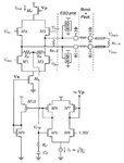
Can anyone highlight the common mode regulation circuit given in the picture is a negative feedback ( CMFB.JPGalways) or an occasional positive feedback?! I am bit confused with the case, if the common mode at the detector output is lower than the reference, then is this not acting as positive feedback?!
Thanks and Regards,
 

Re: Common Mode Regulation in a LVDS Driver

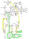
111.jpg

Balancing the differential mode voltage peaks Vn, Vp in yellow and regulating the common mode current in Green.
 

Re: Common Mode Regulation in a LVDS Driver

Thanks for your reply. But my question is if the common mode regulation is only through negative feedback or is this some other special arrangement?! Sorry, I am not clear with that yet.
 
Last edited:

Re: Common Mode Regulation in a LVDS Driver

It's classical negative feedback. Don't know where you see "occasional" positive feedback? Vcm is compared with 1.25V reference by differential amplifier. Three inverting stages in the signal path (M5, M10 ML) make overall negative feedback.
 
Re: Common Mode Regulation in a LVDS Driver

Thanks. my confusion was with the other branch: M6 and Mv
 

Re: Common Mode Regulation in a LVDS Driver

O.K., vp path is inverting as well. Vp is at non-inverting output of differential amp, one inversion by Mv.
 

Re: Common Mode Regulation in a LVDS Driver

Ok. Thanks a Lot. Now Its clear.
P.S. the compensation by Rc and Cc, is this miller compensation?! If so what determines the value of Rc?!
 

Re: Common Mode Regulation in a LVDS Driver

Feedback loop compensation, but parallel RC, not implemented as miller compensation. Selected to achieve sufficient loop phase margin. Notice that common mode output load capacitance creates another pole, thus lag-lead compensation used.
 
  • Like
Reactions: bit_an

    bit_an

    Points: 2
    Helpful Answer Positive Rating
Re: Common Mode Regulation in a LVDS Driver

Wonderful. I think you mean the pole created by the (Bond + Pack) Cap and the termination resistance at the output?! Why do we choose the common mode input for this compensation?! Is this because this is the high impedance node here?! So with minimum cap I can get good phase margin?!
 

Re: Common Mode Regulation in a LVDS Driver

Largest contribution is the LVDS differential pair ground capacitance.
 

Biggest problem in working LVDS or HDMI near or above 1Gbps after smart EQ on the channel in my experience is CMRR from any interference. Adding CM shunt to Gnd capacitance on the balun (SMD CM choke). It can be host specific and sometime just putting my finger over the flat balun reduces the BER sparkles on the video in random locations with high data variations like image edges
 

Status
Not open for further replies.

Similar threads

Part and Inventory Search

Welcome to EDABoard.com

Sponsor

Back
Top