willycat
Newbie level 6
Hi,
i am working on a little project based on a PIC18F4550 and a VNC2 chip, both connected via the SPI interface (in VNC1 compatible mode). I began this project with 2 evaluation boards, one for each chip (the V2EVAL board for the VNC2 chip).
As all worked fine, i decided to go to the next stage by creating a PCB prototype. After soldering all components, i tested the board and faced a problem: that didn't work.
With a debugger, i found that data coming from the VNC2 chip were wrong: they were shifted one bit to the left, losing the seventh bit. Sending data to the VNC2 worked, but not receiving data. I firstly thought about a wrong PCB design and passed much time in this way, but i discovered a strange thing with my scope.
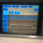
Look at the picture below (signal names are relative to VNC2 chip): It show a read cycle by the PIC. The data sent to the PIC is 0x88 and this is incredible. Instead of beginning to transfer data at the fourth rising edge clock cycle, VNC2 chip begins at the third, ignoring the addr bit ! This doesn't work as expected: according to the datasheet, a read transfer begin with a start bit, a direction bit and an addr bit after what VNC2 transfer the seventh bit of the data, followed by the sixth bit and so... In the point of view of the PIC, writing data works, but not reading.
Now, if i remove the clock cycle relative to the addr bit for a read transfer (not the write transfer), it works fine as expected by my design.
So, without this little modification, it works with the evaluation boards like the datasheet explains; And with this modification, it works with my PCB prototype but not as explain by the datasheet. Same chips, but different behavior. Really ? Not, because there is a little difference: the V2EVAL board has a VNC2 Rev B chip, and my prototype has a VNC2 REV C chip.
Is it possible that the Revision C has a bug that revision B doesn't have (According to FTDI, the only difference is an improvement against ESD protection) ? Or is there really a bug i my PCB prototype design ?
Can someone confirms this bug ?
Thanks,
willy.
i am working on a little project based on a PIC18F4550 and a VNC2 chip, both connected via the SPI interface (in VNC1 compatible mode). I began this project with 2 evaluation boards, one for each chip (the V2EVAL board for the VNC2 chip).
As all worked fine, i decided to go to the next stage by creating a PCB prototype. After soldering all components, i tested the board and faced a problem: that didn't work.
With a debugger, i found that data coming from the VNC2 chip were wrong: they were shifted one bit to the left, losing the seventh bit. Sending data to the VNC2 worked, but not receiving data. I firstly thought about a wrong PCB design and passed much time in this way, but i discovered a strange thing with my scope.
Look at the picture below (signal names are relative to VNC2 chip): It show a read cycle by the PIC. The data sent to the PIC is 0x88 and this is incredible. Instead of beginning to transfer data at the fourth rising edge clock cycle, VNC2 chip begins at the third, ignoring the addr bit ! This doesn't work as expected: according to the datasheet, a read transfer begin with a start bit, a direction bit and an addr bit after what VNC2 transfer the seventh bit of the data, followed by the sixth bit and so... In the point of view of the PIC, writing data works, but not reading.
Now, if i remove the clock cycle relative to the addr bit for a read transfer (not the write transfer), it works fine as expected by my design.
So, without this little modification, it works with the evaluation boards like the datasheet explains; And with this modification, it works with my PCB prototype but not as explain by the datasheet. Same chips, but different behavior. Really ? Not, because there is a little difference: the V2EVAL board has a VNC2 Rev B chip, and my prototype has a VNC2 REV C chip.
Is it possible that the Revision C has a bug that revision B doesn't have (According to FTDI, the only difference is an improvement against ESD protection) ? Or is there really a bug i my PCB prototype design ?
Can someone confirms this bug ?
Thanks,
willy.