Continue to Site

Welcome to EDAboard.com

Welcome to our site! EDAboard.com is an international Electronics Discussion Forum focused on EDA software, circuits, schematics, books, theory, papers, asic, pld, 8051, DSP, Network, RF, Analog Design, PCB, Service Manuals... and a whole lot more! To participate you need to register. Registration is free. Click here to register now.

High current driver for Hi and Low side MOSFET

Status
Not open for further replies.

berger.h

Member level 5
Joined
Sep 30, 2016
Messages
93
Helped
0
Reputation
0
Reaction score
0
Trophy points
1,286
Activity points
2,355
I need drive one high and one low side big MOSFET any as IXFN132N50P3 500V 18nF gate 1,16 ohm gate input resistance .

requirements
Drive current mun 9A may be rather 18A
min 2kV isolated input.

My first idea
2x optoisolator, 2x TC4421 9A mosfer driver and transformer
or
2x optoisolator,, 2x TC4421 9A mosfer driver and 2x isolated DC/DC inverter
or
any something with a higher current and simpler
Which driver is recommended for such large mosfets?
 

Can you use a bootstrap on the high-side? i.e., does the MOSFET turn off periodically so the bootstrap cap can recharge?
 

in general Yes, but i do not know about bootstrap IC with high output current (more than 9A)
 

Whether gate drive transformers are feasible depends on the specific of the circuit. I would only use a GDT if the duty cycle is always near 50%.

Bootstrap drivers are fine so long as you ensure you don't exceed their SOA. Especially their max dv/dt and undershoot on the switching node. Those can kill bootstrapping drivers if not controlled. You can augment their drive capabilities with an external current booster, or even a separate driver following the bootstrap chip.

Safest and most complex option is fully isolated drivers.
 

Whether gate drive transformers are feasible depends on the specific of the circuit. I would only use a GDT if the duty cycle is always near 50%.
Unfortunately not, I need implement Phase shift control

Safest and most complex option is fully isolated drivers.
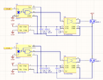
I'm thinking about something like....
2W DC/DC 15V isolatet converter B0515S-2W
12A MOSFET Driver TC4452
but it comes to me complicated and costly
FB.png
 

You didn't mention switching frequencies, thus all power calculations are buried for us.

Gate transformer without active electronic on the secondary looks like the worst idea to me. Paralleling two 9A drivers is an option, the usual solution for high gate current is however discrete transistor buffer.
 

Switching frequency 100kHz +-30kHz
 

Drive current mun 9A may be rather 18A
Maximum gate plateau current for the IXFN132N50P3 is ~8.8 A (assume datasheet conditions, 0.5*VDSS) before breaking its maximum rated dv/dt.
That being said, using a too stronger gate driver might break that limit... care must be taken in that regard.
 

For the isolation look to Silabs isolated half bridge gate drivers which give you isolation and high side drive. It seems you could go with the 1A ones since you need a discrete stage anyway to hit 18A.
 

Unfortunately not, I need implement Phase shift control
Phase shifted bridges are actually one of the topologies that GDTs work well for, since the gates are always driven with 50% duty cycle. Of course you have to make sure leakage inductance is acceptable.

Be wary of some of the low cost isolated DC-DC modules, some of them have high winding capacitance which might cause EMC issues.
 

Right, phase shift is ideal for transformers.

A clever solution I’ve seen is to use a gate drive transformer for both Power and control - rectify its output to generate a dc bus while using its switching transition to control a silicon driver. This would be suitable for phase shift control and scales well to high power.

On the other hand that solution may not actually be smaller or cheaper than a modern DC-DC with an isolated silicon driver.

I like this family from murata which is small, cheap and very low C.

https://power.murata.com/en/nxj1s0505mc.html
 

Thank you all for your comments
especially thank you for the tip On Murata nxj1s0505

I have two options.

1. Full isolated driver. 2x for half bridge or 4x for full bridge
2. GDT drive 1x for half bridge or 2x for full bridge

If I compare pros and cons
FID more expensive (+4$ for each driver 16$ for full bridge) , more precise, 2x higher excitation current
GDT cheaper, easier, lower driving current, size i think both will fit on 50x50 PCB
I really do not know what to decide :thinker:


GDI.png

GDTr.png
 

Gate drive transformer is a solution we use on 10kW phase shift full bridge at 100kHz, 650VDC bus, TIW on suitable toroid, quite low leakage, - you could also augment the gate drive with separate transformers for power if you really want 9 amps of gate drive, then the GD Tx can be signal only...
 

let's get familiar with the 64-bit version of altium 18 , I drew FuL isolated digital GD for full bridge.
The insulation distance is PCB size 55mm x 50mm.
I would also like to try a version with a transformer.

Do you advise the appropriate literature, appnote by which I would like to design a pulse transformer for this purpose?


**broken link removed**
 

The insulation distance is PCB size 55mm x 50mm.
Smallest clearance between channels is below 2 mm, maybe 1.5 mm. That's a bit tight for 500 V working voltage.
 

For insulation distance between channel is crucial two point.
1. Distance between Vout+ and Vout- on the two NXJ1S1212MC. clearance between non isolated part is her 2.5mm. I add slot for extension creepage (perhaps unnecessarily)

2. Distance between S and next G on output terminal blocks (3.5mm ) her is clearance between non isolated part only 2.0mm.

2.5mm is sufficient clearance for 500V for non isolated point according to IPC-2221 . 2.0mm is not safe for 500V , but as working is OK. Solution is simple overcoating with insulating varnish.

500V is in my case sufficient insulating voltage through the channels because 500V is also the max voltage of the MOSFET and isolation barier on safe side is 2.5kV (SI8620BB-B-ISR)

112.png
 
Last edited:

beware with your dcdc module...make sure this is located near to the fet that it is driving....or else you will have a switching node traversing across a potentially large area of pcb, and it may couple into some sensitive traces if you are not careful.
I dont think you can use opto to get up to your high side fet driver since your frequency is too high...use a digital isolator instead, or one of those isolate d gate drivers from infineon........or to be honest, even one of those bootstrap drivers which will level shift your low-side gate drive pulse.....obviously you wont be using the bootstrap part of the bootstrap driver in this case, but who cares.
 

Status
Not open for further replies.

Part and Inventory Search

Welcome to EDABoard.com

Sponsor

Back
Top