Wobbert
Newbie level 3
Dear all,
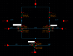
I am designing a down conversion mixer for a wireless transceiver course. I started with just a simple single balanced mixer to get to know the basics. The circuits (mixer circuitry and test bench) are shown below. A mixer multiplies 2 sines. The result should look like this. However I noticed that my output is somewhat different. This is the output of my circuit when feeding it with a (sufficiently large) 900MHz LO and -20 dBm 918MHz RF signal:

You can see that the 18 MHz down converted signal has some strange deformations around the peaks of the signal (marked with a red circle). I increased the power of the RF source, to look if this changes the case, and it only made it worse. When I changed the power of the RF source to 0 dBm, the differential output signal of the mixer became:

As you can see, the deformation/distortion increased significantly. I was thinking about what the cause could be and come up with the following explanation (and that is my actual question): Would it be a fair assumption to attribute this distortion to the (mainly second order, namely the square law) non-linearity of the V to I converter (tail current source MN2)? Because when the input power is increased, the RF MOSFET (MN2) will be driven more out of it's "linear region" (of course this is not strictly non-linear but for small changes in gate voltage it can be assumed as linear) at the peaks of the input signal, resulting in more distortion/deformation at the peaks of the output signal?
Thank you very much in advance!
Test bench:

Analog Circuitry:

I am designing a down conversion mixer for a wireless transceiver course. I started with just a simple single balanced mixer to get to know the basics. The circuits (mixer circuitry and test bench) are shown below. A mixer multiplies 2 sines. The result should look like this. However I noticed that my output is somewhat different. This is the output of my circuit when feeding it with a (sufficiently large) 900MHz LO and -20 dBm 918MHz RF signal:

You can see that the 18 MHz down converted signal has some strange deformations around the peaks of the signal (marked with a red circle). I increased the power of the RF source, to look if this changes the case, and it only made it worse. When I changed the power of the RF source to 0 dBm, the differential output signal of the mixer became:

As you can see, the deformation/distortion increased significantly. I was thinking about what the cause could be and come up with the following explanation (and that is my actual question): Would it be a fair assumption to attribute this distortion to the (mainly second order, namely the square law) non-linearity of the V to I converter (tail current source MN2)? Because when the input power is increased, the RF MOSFET (MN2) will be driven more out of it's "linear region" (of course this is not strictly non-linear but for small changes in gate voltage it can be assumed as linear) at the peaks of the input signal, resulting in more distortion/deformation at the peaks of the output signal?
Thank you very much in advance!
Test bench:

Analog Circuitry:
