Continue to Site

Welcome to EDAboard.com

Welcome to our site! EDAboard.com is an international Electronics Discussion Forum focused on EDA software, circuits, schematics, books, theory, papers, asic, pld, 8051, DSP, Network, RF, Analog Design, PCB, Service Manuals... and a whole lot more! To participate you need to register. Registration is free. Click here to register now.

[SOLVED] Digital Design problem

Status
Not open for further replies.

sweet2shine

Newbie level 4
Joined
Nov 22, 2012
Messages
5
Helped
0
Reputation
0
Reaction score
0
Trophy points
1,281
Activity points
1,310
Hi , from past few days i was stuck in to this diagram which i attached in below. Can any one help me to get out of it.

Thanks in advance
 

Attachments

  • Untitled.png
    Untitled.png
    8.6 KB · Views: 79

Due to these inputs are statically set, it wouldn't make any sense in principle, but assuming that it is really what you saw and also considering that exist a science behind such an implementation, I would try a long shot to say that could be a way to minimize power consumption, or avoid leaving non-used inverter gate inputs floating.
 

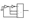
Its a XOR gate. Try to make a truth table using A & B as select inputs of a Mux.

xor.gif
 

In this case, we can assume that the original circuit above would only be the result of some optimization of the synthesizer, using any available unused resource of a macrocell.
 

@Shibin: This could be result of bad synthesis or user have added an inverter pair.
 

Hi Yadav, we can implement ex-or gate in many ways , i think this is the one way to implement but what is the advantage by using this. Can u let me know if possible?
 

Why does anyone think this is an XOR or any specific logic? The drawing has a block with I0-I3 and a Y output, unless the underlying logic of that block is defined, how can anyone make a determination of what that circuit represents?

Besides how can this implement an XOR gate!? There are NO inputs that can be used, they are all connected to static values.
 

Yes, apparently yadavvlsi was thinking laterally, but he may have guessed correctly the (well hidden) intention of the originally post.

Firstly you must read the scribbling on the input of the first inverter as ground symbol. Secondly conclude that the block in the middle should mean a 4:1 encoder, with missing inputs. Finally assume that they are the actual circuit inputs...

Confuse posts like this deserve to be just ignored.
 

Hi, Actually the circuit attached is a 4:1 mux right, now i need to figure out this circuit which resembles the logic gate function?
 

Hi, Actually the circuit attached is a 4:1 mux right, now i need to figure out this circuit which resembles the logic gate function?

This is the problem with posters, that don't know how to ask a question...10 posts and we finally get conformation that yadavvlsi assumed correctly and the rectangle represented a 4:1 mux and the circuit inputs are the mux select lines (not even shown) and the output works just like an XOR gate.

Learn how to ask a question, otherwise you might end up in other member's ignore lists.
 

Status
Not open for further replies.

Part and Inventory Search

Welcome to EDABoard.com

Sponsor

Back
Top