Continue to Site

Welcome to EDAboard.com

Welcome to our site! EDAboard.com is an international Electronics Discussion Forum focused on EDA software, circuits, schematics, books, theory, papers, asic, pld, 8051, DSP, Network, RF, Analog Design, PCB, Service Manuals... and a whole lot more! To participate you need to register. Registration is free. Click here to register now.

Body bias related question

Status
Not open for further replies.

rishabh_31ec

Member level 1
Joined
Sep 13, 2013
Messages
36
Helped
4
Reputation
8
Reaction score
4
Trophy points
1,288
Activity points
1,546
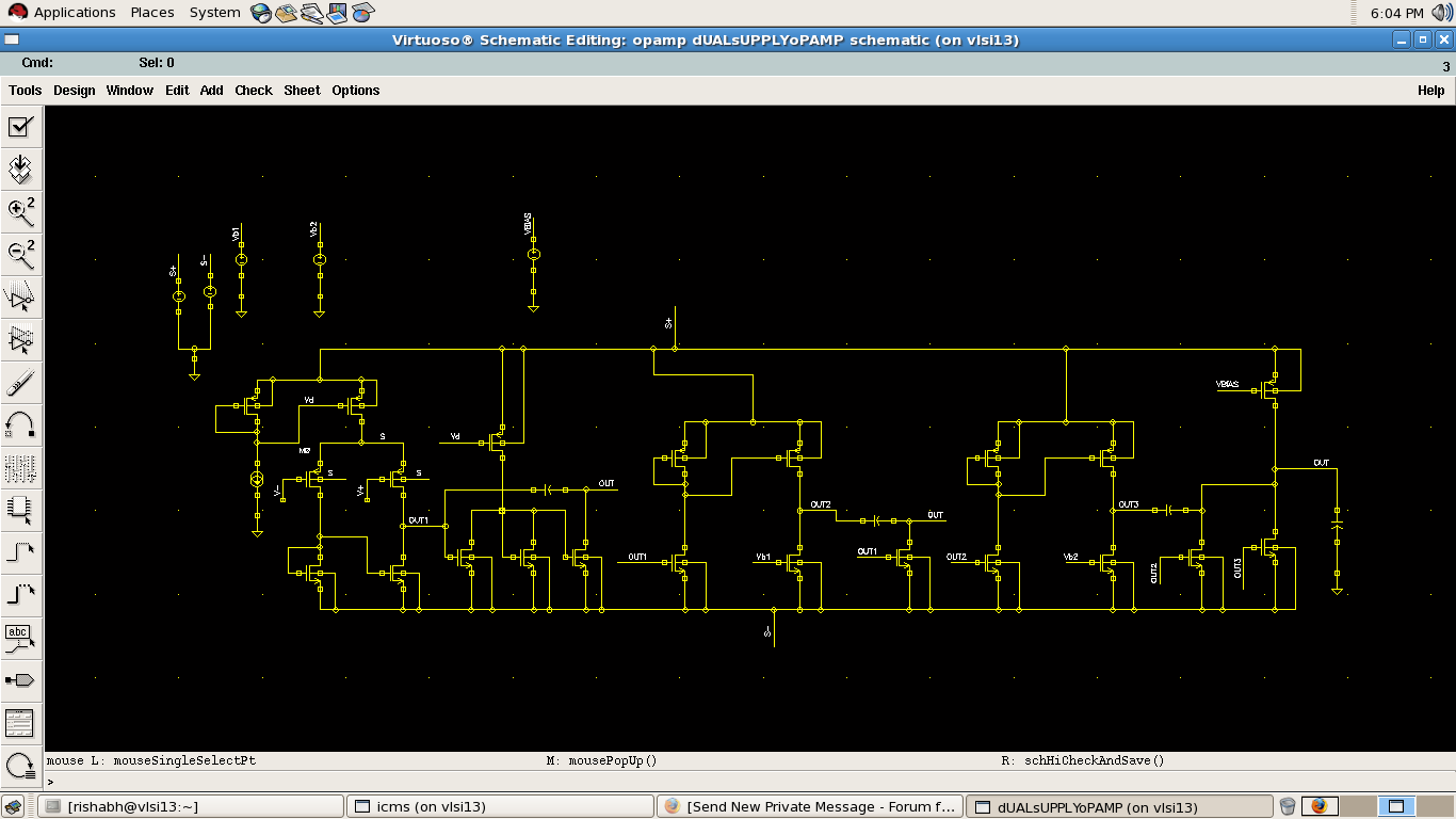
I have designed 4 stage NGCC opamp and provide the body bias for all mos in my design ( + Vdd for body of PMOS , Vss for body of NMOS) but it is a coincidence that source and body remain at same voltage for all MOS except Driver PMOS of first differential pair in which I have shorted the body and source by mistake and complete my designing and I have got all my result properly.
Now I have question whether this is all right or my designing is wrong? I think substrate is common in CMOS technology and provided all pmos share same substrate, so in this case this circuit is wrong, Please clear my doubt regarding validation of my circuit.....


Everything depends to technology. In very old CMOS from 80's the substrate was n-type so each nmos had your own well. The current single well technologies like 0.5-0.25um are nwell nodes with common p-substrate for nmos fets and own nwells for each pmos. Since 0.18um companies start to implementing twin-well and tripple-well options so it's possible to place each pmos and nmos in separate p- or n-well and shorting bulk to sources for transistors lying on diffrent source potentials.

You have to check what kind of devices You have in you technology library or check the process documentation, but the most common all nfets should have bulk shortend to lowest potential, while pfets both to highest or to source.
 
I agree with Dominik, you have to first check which technology you are using. But it shouldn't be a problem as most process now use p-sub so PMOS is definitely in it's own n-well. Therefore, your input PMOS pair should be fine, but at a cost of larger area (you cannot share n-well with other PMOS and n-well separation distance is "huge"). Anyway, check the document first.
 
Status
Not open for further replies.

Part and Inventory Search

Welcome to EDABoard.com

Sponsor

Back
Top