Continue to Site

Welcome to EDAboard.com

Welcome to our site! EDAboard.com is an international Electronics Discussion Forum focused on EDA software, circuits, schematics, books, theory, papers, asic, pld, 8051, DSP, Network, RF, Analog Design, PCB, Service Manuals... and a whole lot more! To participate you need to register. Registration is free. Click here to register now.

[SOLVED] Push-pull emitter follower amp (LTSpice)

Status
Not open for further replies.

PelleS

Newbie level 4
Joined
Feb 8, 2014
Messages
5
Helped
0
Reputation
0
Reaction score
0
Trophy points
1
Activity points
30
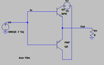
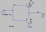
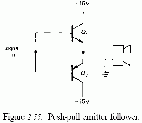
Hi. I'm fairly new to electronics and tried to simulate a circuit from The Art of Electronics in LTSpice. It's supposed to be a simple sound amp. It did not go well, and I am wondering if anybody could help. The circuit is very simple and images are below.

Circuit.png
voltageIn.png
voltageOut.png
 

I don't believe that you got this flawed circuit from the book. Please review the text and/or tell the chapter and page.

- - - Updated - - -

Are you trying to implement this circuit? If so, find the differences!

1324280500_1391859332.gif


- - - Updated - - -

Your transistors need some BIAS. That is a small voltage (~ .8V) to turn on (open up) the base emitter junction. The top transistor needs its base at 1/2 Vcc(V2) + .8V, the lower needs 1/2 Vcc(V1) -.8V.
Yes, the figure 2.55 circuit is used to demonstrate the problem, figure 2.57 is solving it.
 
  • Like
Reactions: PelleS

    PelleS

    Points: 2
    Helpful Answer Positive Rating
I see. Thought the first circuit worked. Thanks for the help :)
 

Attachments

  • Circuit3.png
    Circuit3.png
    4.2 KB · Views: 716
  • Circuit2.png
    Circuit2.png
    4.3 KB · Views: 470

The second circuit does not work as a current amplifier, because the power supply ground connection is missing. You might not realize this in the simulation as the input source will drive the output instead.
 

Circuit3.png

So this is the right way to do it, or am I completely off track?
 

View attachment 101954

So this is the right way to do it, or am I completely off track?
R2 in your circuit is usually the collector of an NPN transistor so it can swing the base of the PNP output transistor completely to ground.
R3 is usually two resistors in series with their junction connected to a capacitor from the output for bootstrapping. Then the base of the NPN output transistor can swing a little higher than the supply voltage. The bootstrapped resistors are a high impedance current source for high voltage gain from the driver transistor.

The two diodes might not match the base-emitters of the output transistors so usually they are replaced with a transistor with adjustable bias.
 

Thank you for helping me out.
 

Status
Not open for further replies.

Part and Inventory Search

Welcome to EDABoard.com

Sponsor

Back
Top