Continue to Site

Welcome to EDAboard.com

Welcome to our site! EDAboard.com is an international Electronics Discussion Forum focused on EDA software, circuits, schematics, books, theory, papers, asic, pld, 8051, DSP, Network, RF, Analog Design, PCB, Service Manuals... and a whole lot more! To participate you need to register. Registration is free. Click here to register now.

What if a wide swing cascode current mirror biased by off-chip circuit?

Status
Not open for further replies.

hyleeinhit

Member level 3
Joined
Aug 11, 2008
Messages
58
Helped
0
Reputation
0
Reaction score
0
Trophy points
1,286
Location
U.S.
Activity points
1,696
Hi,

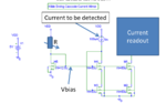
In the attached figure for wide wing current mirror, M1 and M4 are bias by M5 and resistor R. Resistor R is a variableoff chip resistor. Call this as method 1.

In method 2, directly bias M1 and M4 with an off-chip variable voltage generator (two-resistor divider)+buffer.

Which one has better noise performance? And which one is better from your experience?
 

Attachments

  • current mirror2.png
    current mirror2.png
    55.9 KB · Views: 70
Last edited:

Assuming that the bias voltages and current sources are noiseless, it won't change a thing. However, a much more important problem occurs if the method 2 is used, which is the need of a control loop to generate the voltages for M1 and M4. If you leave it as it is, temperature, mismatch or corners might force M1 or M4 into triode region, which again might be undesirable for your operation, not mentioning the increased PCB size and more discrete elements. To establish boundries it is possible to leave a margin, but it is going to be a lot larger than the on-chip load solution since you do not cover the mismatches anymore, therefore you are reducing the swing of a so called wide swing cascode.

To sum up:
1- I don't think noise performance will change. Method 2 might reduce noise if noiseless bias is used because it has a lower number of components on the signal path but again there is no such thing.
2- Fundamental current mismatch, caused by operating point difference between the biasing and the real current source will not change as long as method 1 and 2 provide the same voltage.
3- I really do not see any reason not to use method 1. Method 2 is pure blasphemy if Bob Widlar's idea of "Do not try to match IC elements with discrete elements" taken into account.

If you can tell me what brings you to this question, I might be able to help you more because, please correct me if I'm wrong, the method 2 is doomed to fail obviously both commercially by increasing number of pins and complexity and technically by not being able to compensate the effects of PVT.
 

I am a student and am not developing a product but a prototype. To reduce design time, no voltage reference will be designed on chip, and I consider these two methods to bias the current mirror.

Assuming that the bias voltages and current sources are noiseless, it won't change a thing. However, a much more important problem occurs if the method 2 is used, which is the need of a control loop to generate the voltages for M1 and M4. If you leave it as it is, temperature, mismatch or corners might force M1 or M4 into triode region, which again might be undesirable for your operation, not mentioning the increased PCB size and more discrete elements. To establish boundries it is possible to leave a margin, but it is going to be a lot larger than the on-chip load solution since you do not cover the mismatches anymore, therefore you are reducing the swing of a so called wide swing cascode.

To sum up:
1- I don't think noise performance will change. Method 2 might reduce noise if noiseless bias is used because it has a lower number of components on the signal path but again there is no such thing.
2- Fundamental current mismatch, caused by operating point difference between the biasing and the real current source will not change as long as method 1 and 2 provide the same voltage.
3- I really do not see any reason not to use method 1. Method 2 is pure blasphemy if Bob Widlar's idea of "Do not try to match IC elements with discrete elements" taken into account.

If you can tell me what brings you to this question, I might be able to help you more because, please correct me if I'm wrong, the method 2 is doomed to fail obviously both commercially by increasing number of pins and complexity and technically by not being able to compensate the effects of PVT.
 

Basically, the method 2 is almost never used even while running simulations, therefore I don't think it is a good idea to use it, because of the reasons I've explained. But again I need to point out that I'm not the designer here, you are, and as long as you give solid reasons, it can be used. Simplicity might be one of them but I don't think it is simpler, because you are going to be messing around trying to bias at optimum voltages.

As a result, for this case, it might be good idea to use the method you described as method 1. Actually this is one of the most commonly used method to bias cascodes, for details refer to Design of Analog CMOS Int Cir by Razavi and Intro to Opamp and Comparators by R. Gregorian. For current reference you can just tie a resistor between Vdd and diode connected transistor, it will have the worst PSRR but it will do, as a reference that is technique used in 741 opamp to generate bias.

Again, I must say that there is not really a big difference in things you have mentioned, method 2 is not very good because of practical reasons not because of noise or matching. So I believe this would help you a little but doesn't answer your questions, just challenges their validity :D

Keep working man.
Regards.
 

Status
Not open for further replies.

Part and Inventory Search

Welcome to EDABoard.com

Sponsor

Back
Top