Continue to Site

Welcome to EDAboard.com

Welcome to our site! EDAboard.com is an international Electronics Discussion Forum focused on EDA software, circuits, schematics, books, theory, papers, asic, pld, 8051, DSP, Network, RF, Analog Design, PCB, Service Manuals... and a whole lot more! To participate you need to register. Registration is free. Click here to register now.

How toverifying Simulated Noise Figure and Numerically calculated Noise Figure(NF)

Status
Not open for further replies.

pusparaga

Full Member level 4
Joined
Oct 19, 2013
Messages
197
Helped
4
Reputation
8
Reaction score
4
Trophy points
1,298
Activity points
2,988
Dear Sir,
I have taken the Avago ATF54143 transistor and designed low noise amplifier (LNA), simulated S-parameter and Noise Figure values at 1GHz as follows
S11= 0.581(Mag) and 19.2444(Angle), S21=10.412(Mag) and 179.792(Angle),S12=0.046(Mag) and 139.669(Angle),S22=0.363(Mag) and 51.049(Angle),NF(Noise Figure) = 0.543dB, NFmin=0.36dB.

At 1GHz , transistor ATF54143 has the following noise parameters

Fmin= 0.22dB, Γopt(Gamma Optimum)=0.32(Mag)67.6(Angle), Rn/50= 0.04.

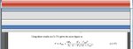
Numerically , we can calculate Noise Figure (NF) using following attachment formula

My question is, how to calculate numerically Noise Figure (NF or 'F' in the attached formula) and Γs( Gamma S). Whatever we are calculating numerical Noise Figure(NF), that should be closer to the simulated noise using the S-parameters as NF=0.543dB. I kindly request someone help me , how to numerical calculated Noise Figure as closer to the simulated noise figure NF=0.543dB.
 

Attachments

  • NOISE_FIGURE_Calculation_Formula.jpg
    NOISE_FIGURE_Calculation_Formula.jpg
    259.1 KB · Views: 165

Honestly I don't understand your question, you want to numerically calculate the noise figure? With the attached formula?
 
johnjoe Sir,
Yes, exactly what you said that is correct. I need to calculate the NOISE FIGURE numerically with the attached formula that should match with the simulated NOISE FIGURE = 0.543 dB(it is shown in the posting # 1) and which value we have to take for GAMMA S(Γs). Please can you help me sir.
 

Sir,
Please someone help me to resolve this difficulty.
 

johnjoe Sir,
Yes, exactly what you said that is correct. I need to calculate the NOISE FIGURE numerically with the attached formula that should match with the simulated NOISE FIGURE = 0.543 dB(it is shown in the posting # 1) and which value we have to take for GAMMA S(Γs). Please can you help me sir.

Gamma(opt) and Fmin can be defined in two ways.Either the manufacturer measures these parameters or they can be found by computed by a SPICE type simulator using with its nonlinear model of the active device.
Becaue Fmin and Gamma(opt) are both intrinsic parameters of the active device and they can not be found easily with a simple linear models and they are depended on pretty complex intrinsic admittances and suseptances.
 
Sir,
What is the way to find out the numerically calculated noise figure cross verify with the simulated noise figure.
 

Dear Sir,
I want to calculate the numerically overall noise figure of circuit "F"( it is shown in the attached formula of the posting #1) using S-parameters, Gamma(opt), noise resistance(Rn), and Fmin of the transistor.
 

Dear Sir,
Some one can help to resolve this problem.
 

Dear Sir,
Some one can help to resolve this problem.

As you have manufacturer's data sheet showing the optimum noise-matching parameters, you were able to ESTIMATE circuit parameters.
For noise figure as low as <1 dB, then you have to build and test the circuit. Make the noise matching circuit variable (inductor and capacitor), and use a calibrated noise-figure meter inside of a screened room to optimize your LNA.
You can spend time by modeling and calculations but adjusting the real circuit is the only proof.
 
Status
Not open for further replies.

Part and Inventory Search

Welcome to EDABoard.com

Sponsor

Back
Top