Continue to Site

Welcome to EDAboard.com

Welcome to our site! EDAboard.com is an international Electronics Discussion Forum focused on EDA software, circuits, schematics, books, theory, papers, asic, pld, 8051, DSP, Network, RF, Analog Design, PCB, Service Manuals... and a whole lot more! To participate you need to register. Registration is free. Click here to register now.

Another lm317 Power Supply

Status
Not open for further replies.

sghr220

Junior Member level 3
Joined
Jun 2, 2009
Messages
31
Helped
1
Reputation
2
Reaction score
1
Trophy points
1,288
Activity points
1,512
Hi guys,

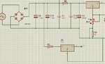
I am building a 10A variable voltage (1.25~50V) power supply using lm317 regulator and the NPN 2sc5200 power transistor as a pass transistor. The transformer output is 48VAC and the circuit is a slightly modified version of the datasheet circuit. When i try to simulate the circuit in Proteus (file attached in this post) i get a fluctuation in the output voltage not really sure where it's coming from. Also should i add an emitter resistor to the output transistor? and if so what is the recommended value and rating?

I really appreciate your help and i am sorry if the subject has been beaten to death in other topics but i really can't find definite answers to my questions elsewhere. :)

ps2.JPG

- - - Updated - - -

Sorry wrong forum, Could the moderators please move the thread to "Analog Circuit Design" thanks.
 

Attachments

  • power supply v2.rar
    17.1 KB · Views: 88

A brief explanation of "fluctuations" would be helpful. Are you talking about permanent oscillations? It may be caused by too much load capacitance.

should i add an emitter resistor to the output transistor?
To achieve what?
 

A brief explanation of "fluctuations" would be helpful. Are you talking about permanent oscillations? It may be caused by too much load capacitance.

A rapid change in the output voltage/current when under load within 1~2 voltage range. How much is too much output capacitance? i am using two output capacitors 220uf and 100nf.

To achieve what?

To prevent thermal runaway or as a temperature compensation.

Thank you for your reply. :smile:
 

The output voltage drops like crazy (about 10~12V) when loading the circuit with a 6.8 ohm power resistor @ 30VDC that's about 4A, now which part is the culprit?
 

To prevent thermal runaway
.. of multiple paralled output transistors. But according to your schematic you don't have it.

How much is too much output capacitance?
I meaned more than in the datasheet example design.

But I compared both designs and found the problem, I think. You added the capacitors C4 and C12 which must not be there. They are introducing a second pole in the loop gain and make the control loop unstable.
 

.. of multiple paralled output transistors. But according to your schematic you don't have it.

Thank you for clarifying that. :grin:

I meaned more than in the datasheet example design.

But I compared both designs and found the problem, I think. You added the capacitors C4 and C12 which must not be there. They are introducing a second pole in the loop gain and make the control loop unstable.

I thought C4/C12 along with R8 form a input filter to the regulator to improve its output performance (i.e reduce high frequency components).

Also please elaborate on the "second pole in the loop gain".

Thanks a lot for your help. :)
 

Forum rules say
Don't bump your thread with useless followups

Did you already try to operate the regulator without the inappropriate low-pass?

If you want to understand the problem in control theory terms, read about loop gain and loop phase margin.
 
  • Like
Reactions: tpetar

    tpetar

    Points: 2
    Helpful Answer Positive Rating
I see that the value of R7 (4700 ohms) is MUCH TOO HIGH and prevents the BD140 transistor from driving the 2SC5200 output power transistor.
Similar circuits in manufacturer's datasheets use an extremely low input current LM195 output device instead of a high input current 2SC5200 power transistor.
The 2SC5200 might work properly if the 4700 ohm resistor is replaced by a piece of wire.
 

Forum rules say


Did you already try to operate the regulator without the inappropriate low-pass?

If you want to understand the problem in control theory terms, read about loop gain and loop phase margin.

You could've spend the same amount of space and letters to answer my questions properly instead of policing the thread.

- - - Updated - - -

I see that the value of R7 (4700 ohms) is MUCH TOO HIGH and prevents the BD140 transistor from driving the 2SC5200 output power transistor.
Similar circuits in manufacturer's datasheets use an extremely low input current LM195 output device instead of a high input current 2SC5200 power transistor.
The 2SC5200 might work properly if the 4700 ohm resistor is replaced by a piece of wire.

Thanks for your answer but if you could take a good look at the circuit and read my first post carefully.

- - - Updated - - -

Forum rules say


Did you already try to operate the regulator without the inappropriate low-pass?

What's inappropriate about it? For a piece of advice to be useful one need to know more than this.
 

At 10A, the minimum current gain of the 2SC5200 transistor is about 22 so its base current must be 10A/22= 455mA.
The minimum current gain of the BD140 transistor at 455mA is about 25 so its base current in the 4700 ohm series base resistor is 455ma/25= 18.2mA and the base resistor will have a voltage drop of 18.2mA x 4700 ohms= 85.5V which causes the circuit to fail.
So remove the 4700 ohm resistor and replace it with a piece of wire.

Of course you're right and i already change that resistor. What i meant in my post (to look carefully) is the input-output voltage difference at the lm317 terminal, will the circuit still works with that nearly 70VDC difference given the max rating of 40VDC for the lm317? Also the 22 ohm resistance at the input of the regulator, is this value correct or does it need to be doubled according to the higher input voltage? (raised current passing through the resistor will cause the pass transistor(s) to always conduct negating the variable output from the regulator)

- - - Updated - - -

I want to add a fan to the power transistor heat sink, the fan specs is 12V/0.2A and will be powered by 7812 regulator to drop the voltage after the bridge and the reservoir capacitors from 70VDC to a suitable input for the 7812 regulator (say 15V) i added a series resistor to the input of the regulator (R5 in the circuit below), any idea how to calculate its value and power rating?
 

Attachments

  • fan.JPG
    fan.JPG
    139.2 KB · Views: 69

You need 11W 275Ω resistor in front of 7812 voltage regulator (70V to 15V).

It will be little heater in this device. :smile:


I dont know what you trying to do with this, but design is not the best. There is LM317HV with max input voltage of 60V but in your case this is not enough. Maybe you should consider usage of newer regulators which allow higher voltages (linear and switcher regulators).

I will consider design with switcher regulator.

Plus take in consideration power dissipation of parts (transistor), when you have big voltage difference (Vin-Vout) and high current, your device will dissipate high power. What you expect from this device?


Best regards,
Peter
 

You need 9W 225Ω (220Ω) resistor in front of 7812 voltage regulator (60V to 15V).

Hi Peter, thanks for your input but could you elaborate on how you calculated these values. :smile:

I dont know what you trying to do with this, but design is not the best. There is LM317HV with max input voltage of 60V but in your case this is not enough. Maybe you should consider usage of newer regulators which allow higher voltages (linear and switcher regulators).

The lm317 used is floating so it sees only an input-output difference within its ratings (40V).
 

Hi Peter, thanks for your input but could you elaborate on how you calculated these values. :smile:


Calculation:

Input voltage 70V
Needed voltage 15V (at least 3V higher then 12V because 7812 regulator)
Current 0,2A (Raw without other currents of regulator IC,...)

R = 70V - 15V = 55V / 0,2A = 275Ω

P = I²R = (0,2A x 0,2A) x 275Ω = 11W


The lm317 used is floating so it sees only an input-output difference within its ratings (40V).


Someone has to pay the bill, bypass transistor will pay. :)


Best regards,
Peter

;-)
 

Calculation:

Input voltage 70V
Needed voltage 15V (at least 3V higher then 12V because 7812 regulator)
Current 0,2A (Raw without other currents of regulator IC,...)

R = 70V - 15V = 55V / 0,2A = 275Ω

P = I²R = (0,2A x 0,2A) x 275Ω = 11W

Thanks a lot for your help. :grin:
 

Power dissipation for 5V and 3A on output will be 50V-5V=45Vx3A=135W.

2SC5200 can allow maximum 150W at Tc=25C.

Theoretically on longer you can use 10A from this design only if output voltage is set around 40V.
For voltage bellow 40V current should be decreased, because power dissipation is increased on bypass transistor.


All depends what currents at what voltages you will need to use, and you need to know what you can expect from this design.

Always you can add one more transistor in parallel to increase dissipation power. Also its good to implement maximum power and over temperature protection and signalisation or smoke is inevitable in some delicate situations.


Best regards,
Peter

That's a very good description of the problem. What the max. output current expected at 18v? :grin:
 

That's a very good description of the problem. What the max. output current expected at 18v? :grin:

I try to tell you from first post, this should be first item for discussion before starting to make design. :)

50V - 18V = 32V (voltage difference)
32V x 3A = 96W (power dissipation) - count up to 100W power dissipation for that case with good cooling.

If you have more then 50V of input voltage, this situation is worse.


This is situation when you should start to think about switching psu. :)


Best regards,
Peter

So Peter i can't thank you enough, what modifications do you suggest for the above circuit? or do you suggest another designs? (no SMPS please, it is noisy as hell and also the components is hard to come by).
 

Status
Not open for further replies.

Similar threads

Part and Inventory Search

Welcome to EDABoard.com

Sponsor

Back
Top