VLSI_Learner
Member level 2
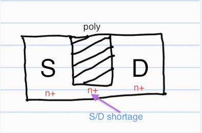
1. If there is no poly cap, then poly ends (up/down) will align with diffusion edges. Why it is not done? What problem it might create?
2. If poly is smaller than the diffusion (device) width, what problem it might cause?
For reference please see the picture.

2. If poly is smaller than the diffusion (device) width, what problem it might cause?
For reference please see the picture.