btv_murthy
Full Member level 3
Dear Sir,
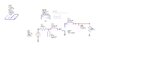
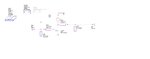
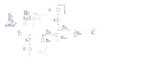
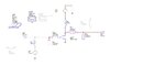
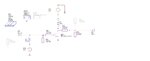
I designed simple low noise amplifier for 2DB Noise Figure and Maximum gain ( given in David .M.Pozer book Example 11.5 page no559 third edition)for the following S-parameters at 4GHz, used FHX35LG HEMT Transistor.
S(1,1) S(2,1) S(1,2) S(2,2)
mag angle mag angle mag angle mag angle
4GHz 0.6 -60 1.9 81 0 0 0.5 -60
F(min) = 1.6 dB, Noise Resistance of transistor = 20 Ohm, optimum reflection coefficient of transistor = mag 0.62 angle 100
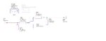
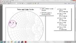
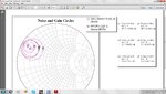
I used AWR MWO software tool and simulated , didn't get proper gain and noise figure circles. Here with I am attaching the desired noise figure circle and gain circle and obtained NF circle and gain circle. I don't know where I am doing mistake, please can you help me get the desired NF circle and maximum gain.
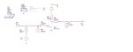
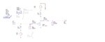
I designed simple low noise amplifier for 2DB Noise Figure and Maximum gain ( given in David .M.Pozer book Example 11.5 page no559 third edition)for the following S-parameters at 4GHz, used FHX35LG HEMT Transistor.
S(1,1) S(2,1) S(1,2) S(2,2)
mag angle mag angle mag angle mag angle
4GHz 0.6 -60 1.9 81 0 0 0.5 -60
F(min) = 1.6 dB, Noise Resistance of transistor = 20 Ohm, optimum reflection coefficient of transistor = mag 0.62 angle 100
I used AWR MWO software tool and simulated , didn't get proper gain and noise figure circles. Here with I am attaching the desired noise figure circle and gain circle and obtained NF circle and gain circle. I don't know where I am doing mistake, please can you help me get the desired NF circle and maximum gain.