Continue to Site

Welcome to EDAboard.com

Welcome to our site! EDAboard.com is an international Electronics Discussion Forum focused on EDA software, circuits, schematics, books, theory, papers, asic, pld, 8051, DSP, Network, RF, Analog Design, PCB, Service Manuals... and a whole lot more! To participate you need to register. Registration is free. Click here to register now.

[SOLVED] LVS error: MALformed device - ASSURA

Status
Not open for further replies.

palmeiras

Full Member level 6
Joined
Feb 22, 2010
Messages
375
Helped
61
Reputation
122
Reaction score
50
Trophy points
1,308
Location
South America
Activity points
4,199
Hi guys,

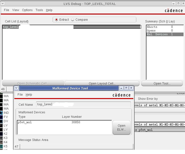
The following error appears when running LVS with ASSURA:
"malformed device PMOS”"– for IBM 130 nm
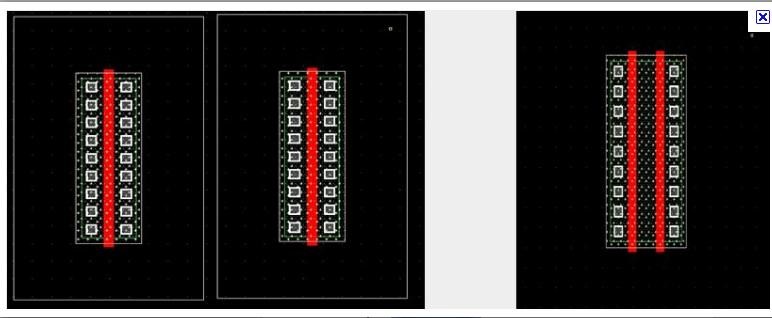
It appears for my differential pair: M1 (multiplicity = 8) and M2 (multiplicity = 8).
The first 8 devices are abutted, as well the others 8 – performing a centroid configuration.
I have already used M1<0:7> or put all devices in parallel. The tool still points this error.
It seems that it does not liked of the abutment.
Does anyone know how to solve this error?

Thanks in advance,
 

Could you please upload a screenshot of the error?Where does it appear : at the LVS Debug Environment or at the dynamic report that you can watch when LVS is running?
Additionally what kind of devices do you use (regular transistors,RF,etc.)?
 
The tool has some logic that "recognizes" device type based
on features. It may not (say) like a complex body or gate shape,
whatever. If the devices are recognized with finite spacing and
only fault when abutted, then you should look at the features
which now overlap for the issue.

That or you could just eat the extra 1-2um and get past it.
 

Hi jimito!
Thanks for your reply!
I´m using the LVS Debug Environment. I can watch the LVS running, and when the results appear, all errors are ignored. The only message that appears is "malformed device PMOS".
I guess this happen because I´ve abutted the devices. But this function should work fine. I am using regular devices.
I´ll take a print screen of this error.
 

Upload the screenshot to assist you further.Can explain further the term "abutted devices"?I have never heard about this before and i need some explanation to get into the things you have done ;-)


---------- Post added at 00:50 ---------- Previous post was at 00:46 ----------

This problem happens after using abutment transistor. Jimito, do you have a suggestion?

Thank you!
 

What does the term "abutment transistor" mean?Can you show a photo of this implementation?
 

Abutment is some thing like described by this figure. But in my case, I´ve kept the contat in the shared terminal.


Ok,i was suspecting like this for the term abutment but i wanted a confirmation.To my knowledge this implementation is called interdigitization.

I think that you have connected in a wrong way the sides of some transistors,that is a D (drain) is connected to S (source) of the other transistor or vice versa and that's why you get this error.
 

Abutment is some thing like described by this figure. But in my case, I´ve kept the contat in the shared terminal.


It looks like the body terminal (mapped to well) is present in the layout with two separate transistors (on the left), but is missing in the layout with two abutted transistors (on the right).
Check the body terminal - its presence is usually required for proper MOS transistor recognition.
 

Hi guys!!
Thanks for the replies. The last figure I´ve uploaded was only to give an example.
I´ve replaced my transistors without using multiplicity, but in fact, in parallel. And the tool recognizes it.

Best regards,
 

Status
Not open for further replies.

Part and Inventory Search

Welcome to EDABoard.com

Sponsor

Back
Top