Continue to Site

Welcome to EDAboard.com

Welcome to our site! EDAboard.com is an international Electronics Discussion Forum focused on EDA software, circuits, schematics, books, theory, papers, asic, pld, 8051, DSP, Network, RF, Analog Design, PCB, Service Manuals... and a whole lot more! To participate you need to register. Registration is free. Click here to register now.

NMOS bulk connection - (2 wells: twell inside nwell)

Status
Not open for further replies.

sw0ws1

Junior Member level 1
Joined
Jul 15, 2010
Messages
19
Helped
2
Reputation
4
Reaction score
1
Trophy points
1,283
Activity points
1,428
My problem is the bulk connection of nmos because my nmos is located in two wells, twell and nwell,
the twell is located inside the nwell (as i upload here) ,my question is

1-i think the twell is the bulk of the nmos/is this true??
2-how i connect the bulk of nmos(twell) to its source ( i have no contact named
M1_twell but i have M1_Nwell, M1_poly, M1_Pdiff, M1_ndiff )??
3-when i try to put a M1_pdiff contact in the twell ,it causes DRC errors (like diff to diff min disance, ..)???
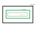
ss.png

thanks in advance
 

Re: NMOS bulk connection

What's doping type for twell? P-type or N-type?
 

Re: NMOS bulk connection

logically i think the doping of twell is p-type to form NMOS but i don't know this is true or not??
 

Re: NMOS bulk connection

My problem is the bulk connection of nmos because my nmos is located in two wells, twell and nwell,
the twell is located inside the nwell (as i upload here) ,my question is

1-i think the twell is the bulk of the nmos/is this true??
2-how i connect the bulk of nmos(twell) to its source ( i have no contact named
M1_twell but i have M1_Nwell, M1_poly, M1_Pdiff, M1_ndiff )??
3-when i try to put a M1_pdiff contact in the twell ,it causes DRC errors (like diff to diff min disance, ..)???

View attachment 59101

thanks in advance

Hi sw0ws1,

you seem to be trying to generate a triple well NMOS (also known as a deep-N-well NMOS); in all PDKs I have dealt with, the N-well layer is a ring partially overlapping TW (not a rectangle), are you sure your process requires using a rectangle?

Also usually the TW identifies the deep (N)well implant that creates the isolated P-well for the NMOS: basically the isolated pwell (that some foundries call RW) can be thought as a box whose bottom face is TW and whose side faces are NW (the top face is the silicon surface)

When contacting the body of the isolated NMOS you just need a p-contact to RW (M1_Pdiff in your case), of course you need to make sure you have enough room to avoid DRC violations
 

Re: NMOS bulk connection

Please note NMOS' bulk will be P-type always.
 

thanks for all of u the problem is solved
i used M1_pdiff contact and add new twell and nwell to avoid the DRC errors....
thanks again
 
I just hope you understand the structure or you might end up with incorrect LVS....
 

Status
Not open for further replies.

Part and Inventory Search

Welcome to EDABoard.com

Sponsor

Back
Top