Continue to Site

Welcome to EDAboard.com

Welcome to our site! EDAboard.com is an international Electronics Discussion Forum focused on EDA software, circuits, schematics, books, theory, papers, asic, pld, 8051, DSP, Network, RF, Analog Design, PCB, Service Manuals... and a whole lot more! To participate you need to register. Registration is free. Click here to register now.

Transistor bias question ?

Status
Not open for further replies.

crazyjohn

Junior Member level 2
Joined
Dec 4, 2010
Messages
24
Helped
0
Reputation
0
Reaction score
0
Trophy points
1,281
Activity points
1,467
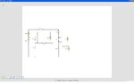
Ive got a npn transistor circuit set up in a emitter amplifier configuration.Ive set the base voltage at 5v though the voltage divider and set RE to drop the remaining 4.2v at 50ma which should control IC and IE current.

The problem is how do i calculate the value of r1 or r2 of the voltage divider so that it will output 5v even after being connected to the transistor base and RE ?

How is vbe recalculated when deterrent loads are placed between v+ and the collector ?
 

Attachments

  • transistor bias.JPG
    transistor bias.JPG
    71.4 KB · Views: 79

You would normally design for a current in the bias chain 10 times the lowest base current or more. So, with 50mA of base current if you assume hfe of 100 then the base current would be 0.5mA. So, you would maybe use 5mA for the bias resistor chain. This will be affected by the base current but you probably don't want 50mA in the bias chain - it would consume a lot of current and make the input impedance low. So, after choosing your base resistors you can either tweek one of the values to correct for the base current or adjust the emitter resistor.

You could do the calculation properly which involves solving the equations for the two resistors and the base current. So, for example, 5mA through the resistor from VCC and 4.5mA down the lower resistor and 0.5mA. Down the base.

I hope that makes sense!

Keith
 

Crazyjohn,

Keith's reply about 10 times ibe is the usual solution for amplifiers etc that do no have a significant load and are broadly class A.

However 50mA of ice suggests you have a low load impeadence in which case the setting of vbe may be not where you would expect to get the desired output DC conditions.

Depending on what your design is for you may need to model the load on the collector first either in a cad package such as spice or by the old "**** and see" method.

As a very rough rule of thumb assume Vc never goes above 90% V+ rail and not below Ve+10% of rail (ie the transistor is always in conduction. And thus the DC bias point of VC is ~0.5% of that value.

Thus the easy way to determin the values of the base bias resistors is to first determin the corect value of Re to give not just the desired current but alow the desired swing on the collector.

Having done this with an appropriate DC load (if not AC coupled) you need to raise Ibe to give the corect value of Vc.

To do this use a variable resistor from the bias rail (if not from the V+ rail). to the base with no other connection to the base (that is it is a variable resistor not a potentiometer). Adjust its value so that Vc is at the correct value and measure Vb to ground (or the other base biase rail).

Take the veriable resistor out of circuit and use a resistor between one third and one tenth of its value to the base and another resistor of appropriate values to give the correct Vb and thus Vc value.

Hope that helps,

Clive.
 
  • Like
Reactions: arthur0

    arthur0

    Points: 2
    Helpful Answer Positive Rating
Can someone give me another example of choosing r1,r2,re so that the bias voltage divider delivers a vout with the loading effect in mind at a particular voltage and current?
 

Status
Not open for further replies.

Similar threads

Part and Inventory Search

Welcome to EDABoard.com

Sponsor

Back
Top