jimito13
Advanced Member level 1
Hello all,
I will try to describe my problem the better i can.I have an op-amp design that consists of several cells (main opamp,gain boosters,cmfb,biasing).I have created the layout of all the above cells and i pass successfully from DRC and LVS runs (clean runs,no errors no warnings).The last step is to perform the parasitics' extraction and run post layout simulations.Well,here things become a little bit strange...Before i describe my problem in depth i must say that my design kit is IBM's cms9flp and the versions of cadence virtuoso and assura are IC6.1.3.500.13 and 3.2_USR2_HF11 respectively.
I run LVS for each cell successfully (clean results) and then i run successfully as well the assura QRC run (no errors-no warnings) for all my cells and the result is the well known message of assura with the av_extracted view's name and location in the library.
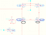
Next step is to simulate the av_extracted views.For this i create a schematic with all the above cells interconnected as symbols and i use the av_extracted declaration under Environment submenu of ADE L.
I run DC analysis at first and here is my issue.The currents in all branches of the circuit are far away from the designed values.From a quick thought you can say that i made mistake in transistor sizes during layout but this should be reported by LVS but in any case i double checked this by myself to be absolutely certain.Second thought is that i have not calculated correct the widths of all metals that make the interconnections in the design,i double checked this as well according to pdk's rules for metals and viases.With a more careful view in the values of the currents that dc analysis resulted i noticed that all of them are divided by the product (m*nf),where m is multiplicity and nf number of fingers!Looking at the vdd symbol i see that my circuit consumes X mA but if i add all the currents from the subcells i do not ever reach X/4 mA,so i ask myself where is the rest of the current consumed?!Another strange thing is that even though that all currents are wrong calculated the biasing voltages from the current mirrors are exact to the design values...
Has anybody else come up with such an issue with this or another IBM's pdk??Do you think that i should report this straightly in IBM's support??
PS. It is urgent for me since tape out date is close!!
Thanks in advance for any helpful answer.
I will try to describe my problem the better i can.I have an op-amp design that consists of several cells (main opamp,gain boosters,cmfb,biasing).I have created the layout of all the above cells and i pass successfully from DRC and LVS runs (clean runs,no errors no warnings).The last step is to perform the parasitics' extraction and run post layout simulations.Well,here things become a little bit strange...Before i describe my problem in depth i must say that my design kit is IBM's cms9flp and the versions of cadence virtuoso and assura are IC6.1.3.500.13 and 3.2_USR2_HF11 respectively.
I run LVS for each cell successfully (clean results) and then i run successfully as well the assura QRC run (no errors-no warnings) for all my cells and the result is the well known message of assura with the av_extracted view's name and location in the library.
Next step is to simulate the av_extracted views.For this i create a schematic with all the above cells interconnected as symbols and i use the av_extracted declaration under Environment submenu of ADE L.
I run DC analysis at first and here is my issue.The currents in all branches of the circuit are far away from the designed values.From a quick thought you can say that i made mistake in transistor sizes during layout but this should be reported by LVS but in any case i double checked this by myself to be absolutely certain.Second thought is that i have not calculated correct the widths of all metals that make the interconnections in the design,i double checked this as well according to pdk's rules for metals and viases.With a more careful view in the values of the currents that dc analysis resulted i noticed that all of them are divided by the product (m*nf),where m is multiplicity and nf number of fingers!Looking at the vdd symbol i see that my circuit consumes X mA but if i add all the currents from the subcells i do not ever reach X/4 mA,so i ask myself where is the rest of the current consumed?!Another strange thing is that even though that all currents are wrong calculated the biasing voltages from the current mirrors are exact to the design values...
Has anybody else come up with such an issue with this or another IBM's pdk??Do you think that i should report this straightly in IBM's support??
PS. It is urgent for me since tape out date is close!!
Thanks in advance for any helpful answer.