dirac16
Member level 5
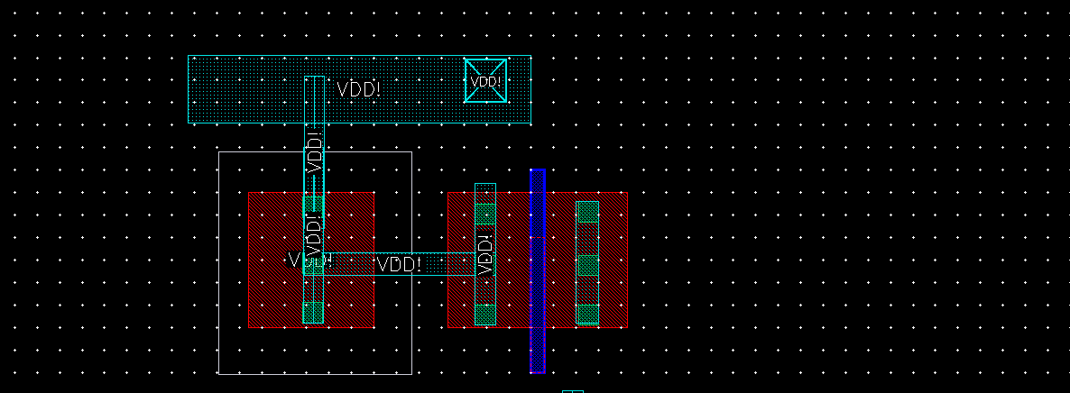
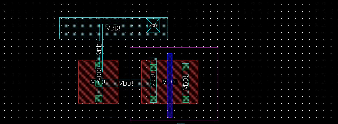
I am trying to lay out a simple CMOS inverter. I successfully drew the layout for NMOS. However for PMOS transistor I got a strange problem: The problem is when I surround PMOS active region with PP layer then all of a sudden the drain and oxide diffusion layer get connected to VDD! That is a pretty strange behavior and don't know why it happens. The following two pictures show PMOS layout before and after adding PP layer.


If you also look even more carefully you could notice that the NP layer surrounding the bulk terminal has also made the oxide short to VDD! So the issue is not peculiar to PP layer only.
If you also look even more carefully you could notice that the NP layer surrounding the bulk terminal has also made the oxide short to VDD! So the issue is not peculiar to PP layer only.
Last edited: