ja2bo2t
Newbie level 4
Hi All,
I'm in the middle of a mixed-signal design project using the TSMC 0.35um 2P4M process. I've done some chip layouts in 0.5um before during undergrad, but this is my first time using 0.35um. I have a few questions and concerns:
I appreciate any thoughts and comments.
I'm in the middle of a mixed-signal design project using the TSMC 0.35um 2P4M process. I've done some chip layouts in 0.5um before during undergrad, but this is my first time using 0.35um. I have a few questions and concerns:
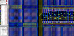
- I've created some custom digital standard cells to do the limited digital logic that we have (just thought it would be easier). In filling in the extra space I've added decoupling PIP capacitors in between the rails (see attachment). Will the large continuous amount of Poly1 (shown in blue) cause problems with the gate poly nearby? Some of the larger empty areas are up to 400um x 400um; I'm concerned that the resolution of the gate poly on the edges of these large capacitive regions will be reduced.
- I have read in many places that using double vias throughout the design can increase yield in smaller technologies. Is 0.35um small enough to worry about connection problems for single vias on digital connections (whether they are metal to metal, metal to poly, or metal to diffusion)?
- I have also read that using minimum width and spacing for metal routing can cause yield issues for long traces. I have been using 0.6um width/0.65um spacing (design rule minimums are 0.6um width/0.5um spacing) for traces up to ~5000um in digital busses (see attached); will this cause problems in 0.35um?
- In connecting the digital parts of the circuit (outputs from SRAM latches) to analog switches, what is the typical way of handling the grounds? A basic description would be an array of SRAM directly connected to analog switches (much like an FPGA but the switches are analog) that are part of a very noise sensitive analog amplifier. The SRAM will not be written to during normal operation, but there will be digital operation and thus some noise on the digital VDD and VSS lines (currently it is conceived to use separate analog and digital supply rails). Is it preferential to make small ground connections at the locations of the switches, or to connect the grounds off chip. The main tradeoff that I see is the creation of the large loop that connecting grounds off chip would make in comparison to the noise that will be coupled from the digital to analog supplies.
I appreciate any thoughts and comments.
")