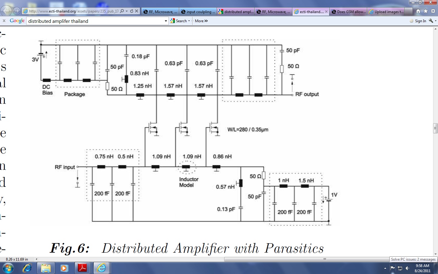
Continue to Site

Welcome to EDAboard.com

Welcome to our site! EDAboard.com is an international Electronics Discussion Forum focused on EDA software, circuits, schematics, books, theory, papers, asic, pld, 8051, DSP, Network, RF, Analog Design, PCB, Service Manuals... and a whole lot more! To participate you need to register. Registration is free. Click here to register now.

input coulpling capacitor in LNA

Status
Not open for further replies.

lna.fyp

Newbie level 6
Joined
Jun 4, 2011
Messages
13
Helped
0
Reputation
0
Reaction score
0
Trophy points
1,281
Activity points
1,366
ive designed a LNA for 0.1G to 3G, i havent added input couplign capacitor and the simulations results are just fine, the problem is when i add input coupling cap, the gain becomes negative and all the results deteriote. i wanted to know in this case can i use an external coupling capacitor which will not be considered in simulations? and also is it necessary to add coupling capacitor inthe schematic and layout
 

Any capacitor have a SRF (resonant frequency) and a parasitic inductance, that you have to take in consideration during your simulation.
Ideally is to use in your simulation the S parameters of the capacitor provided by the manufacturer.
 
Any RF active circuit needs coupling capacitors. but some LNA's having inbuilt coupling capacitors which may need a simple inductor circuit at the input for matching.
if not, as said above select the capacitors whose SRF is higher that your frequency of operation. change the position of coupling cap after the matching circuit and see.
negative gain sounds like circuit is not stable, check for stability also. keep ideal caps first and simulate the circuit and replace the ideal with capacitor models and optimize.
 
what do u mean by having inbuilt couplng cap?simple inductor circuit??r u referring to some L-matching n/w?? ur answer is not very clear, plz if u can elaborate on it further. and have a look atthis ciruit, it doesnt have any coupling capacitor , so is this design okay?
**broken link removed**

this isnt my circuit , but it also doesnt have any coupling capacitor

and negative gain occurs only after i add a coupling capactior, otherwise my circuit works perfectly..fully stable
 

see attached chip as caps inside.
 

Attachments

  • Screenshot-AV02-0322EN.pdf - Adobe Reader-1.png
    Screenshot-AV02-0322EN.pdf - Adobe Reader-1.png
    121.5 KB · Views: 147

sir, we are designing an LNA chip..by built in capacitor r u referring to an on chip capacitor?? we already are referring to an on chip capacitor...
actually we are very basic level designers..designing LNA as a part of our university project..so we are very sorry if our questions seem irritating but it wil be a great help if u could guide us..cuz we are in a big fix over this issue
 

An input coupling capacitor blocks DC. On the other hand, in order to compensate such capacitor a series inductor is used, and it allows to set input operating frequency, but it depends on LNA topology. Which topology are you using?. For example, an inductive source degeneration topology allows to improve linearity and common-gate topology has better bandwidth.
 
  • Like
Reactions: rbh

    rbh

    Points: 2
    Helpful Answer Positive Rating
see page 7 of link 1 document to avoid RF current getting grounded and to reduce noise due to a pole at the output a series inductor is used at input with out a coupling capacitor
from page 10 of link 2 document :Gate to source capacitance becomes significant and an inductor is used to nullify gate to source capacitance and use it for matching. so a coupling cap can be avoided for CMOS common gate LNA's.
the above are for CMOS cascode LNA designs only.
link1: https://citeseerx.ist.psu.edu/viewdoc/download?doi=10.1.1.152.6121&rep=rep1&type=pdf
link2: https://www.qsl.net/va3iul/LNA design.pdf
 
i am designing a distributed cmos casode lna from 0.1G to 2.7G problem is that when i add a coupling capacitor even in the basic distrbuted topology , gains s21 becomes negative.

---------- Post added at 17:17 ---------- Previous post was at 17:02 ----------

can coupling cap only be ignored in case of common gate? what about common source, im making distributed amplifer which is common source . whenever a capacitor is added even in the basic topology of distributed amplifer without any ither thing added , the gain is negative!
 

with ideal capacitor. and yes in simulation. im using cadence.
 

Complex S21 will be a negative value due to the circuit's phase reversal of course. Or are you referring to S21 magnitude (in db)?
 

In this case, I expect either insufficient transistor gm or output saturation. Did you determine gm? What is transistor Id?
 

I would expect a gm > 30 mmho (mS) for this Id value with Vgs of 1 V. It should be listed in the Cadence analysis. A gain of -20dB refers to a gm < 2, which sounds unlikely. So there must be some circuit error.
 

In circuit refereed as fig6, are parasitic losses included as if they were components. It is a symbolic signal schematic with 3 cap, 3 res and 3 transistors specified. It is a typical schematic where only parameters needed for RF simulation are included, not equal with a real circuit.
As there is no DC design, are these components not specified. Input/Output of this circuit can not be loaded by a DC load as that would affect DC bias.
Serial cap at input and output are therefore assumed as it is a DC voltage at these pins.
A serial cap at input, of any normal value, can not cause the problem you describe, at least not in this circuit. It is more likely related to simulation setup.
 
Last edited:

Status
Not open for further replies.

Similar threads

Part and Inventory Search

Welcome to EDABoard.com

Sponsor

Back
Top