Welcome to our site! EDAboard.com is an international Electronics Discussion Forum focused on EDA software, circuits, schematics, books, theory, papers, asic, pld, 8051, DSP, Network, RF, Analog Design, PCB, Service Manuals... and a whole lot more! To participate you need to register. Registration is free. Click here to register now.
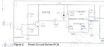
It seems that C2, R1 and Q1 prevent from pushbutton bouncing.
R2, C1 and the internal pull-up of manual-reset input determine the reset pulse duration once the pushbutton was pushed down.
D1 clamps the reset input when C1 discharges through R2.
IMHO this circuitry may be useless due to the EM6325C has internal debouncing, so all you need is connecting the pushbutton from GND to the manual reset input.
The only difference should be that, in the last case, the reset output will keep active until you release the pushbutton.
What if I remove that push button.Actually i have another circuit without that push button too. But it doesnot make sense for me to use a transistor before a reset circuit... An why C1 is reverse baised. As i know if you reverse bais a capacitor it will get blown up.
Yes, you may remove the pushbutton and all the circuitry around it, but manually reset will not be possible.
C1 is not reversed.
If you take a look at the datasheet of the EM6325, you'll find an internal pull-up resistor in the manual reset input, so that when Q1 is "ON" the minus pin of C1 falls to ground, and the plus pin of C1 is tied to VCC through the internal pullup. When Q1 is "OFF" both minus and plus pins are connected to VCC through R2 and pull-up respectively. D1 gives C1 a discharge path when Q1 switch to OFF, clamping the manual reset input to [VCC + VD1forward].
Thanks for the reply,but i have some more querys.Since,when Q1 is "ON" the minus pin of C1 falls to ground, and the plus pin of C1 is tied to VCC through the internal pullup. then how does MR(Low) gets active. In both cases,It will have some voltage at it pin.
Do reply.
This site uses cookies to help personalise content, tailor your experience and to keep you logged in if you register.
By continuing to use this site, you are consenting to our use of cookies.