Continue to Site

Welcome to EDAboard.com

Welcome to our site! EDAboard.com is an international Electronics Discussion Forum focused on EDA software, circuits, schematics, books, theory, papers, asic, pld, 8051, DSP, Network, RF, Analog Design, PCB, Service Manuals... and a whole lot more! To participate you need to register. Registration is free. Click here to register now.

Capacitance in parallel to VCO input on PLL loop filter

Status
Not open for further replies.

kalbun

Full Member level 2
Joined
Oct 2, 2010
Messages
134
Helped
37
Reputation
74
Reaction score
36
Trophy points
1,318
Location
Firenze, Italy
Activity points
2,114
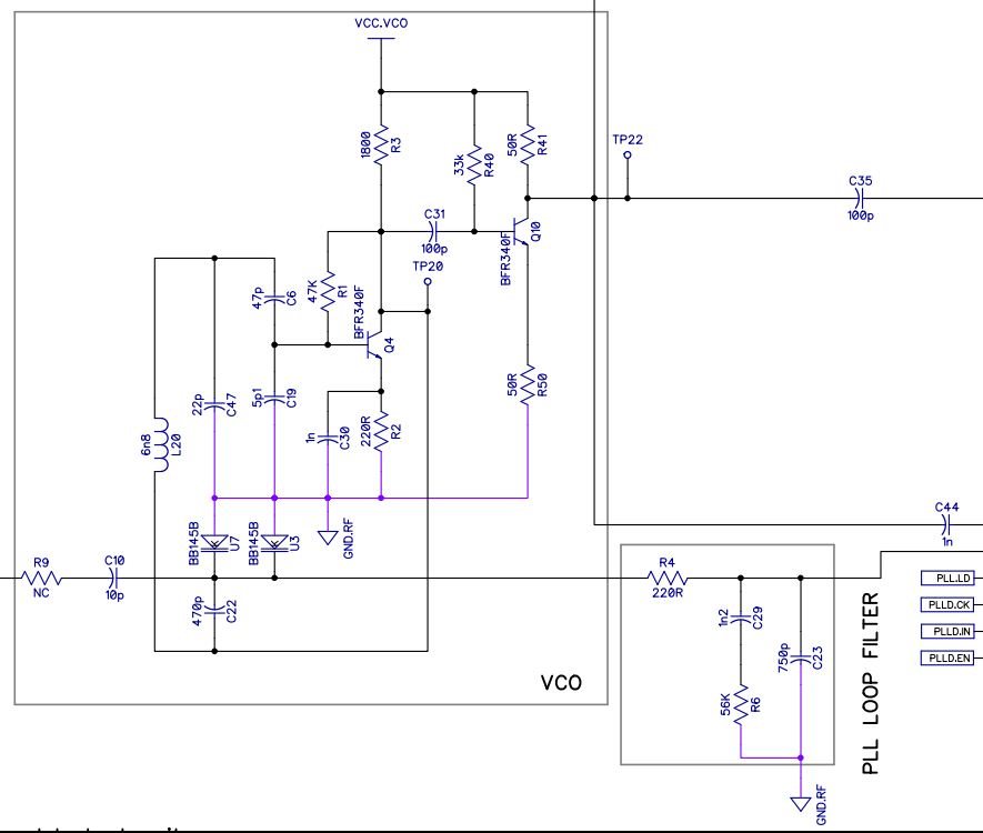
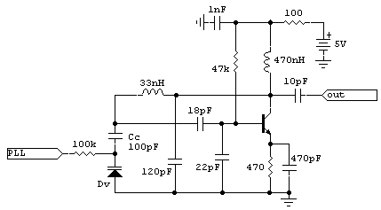
In a 3rd order PLL loop filter, the last capacitor is put in parallel to the VCO input.

But doing so, aren't we modifying the VCO frequency range? Or must this capacitor be taken into account at design stage?

Maybe an RF engineer will consider this as an idiot's question, indeed RF is not my job (nonetheless for various reasons I am in strong need to learn some RF basis 8O)
 

You seem to be confusing the ports on your VCO. The VCO has an RF output port, where RF/Microwave frequencies come out.

It also has a tuning voltage input port. NO RF energy comes out of that port, so adding a capacitor to ground there does absolutely nothing to limit the tuning range of the RF portion of the oscillator. (You do have to make sure that the control loop does not go unstable due to the capacitance you are adding!).
 

Hello biff44,
my doubt is exactly this.
I know that the signal coming from the charge pump is feeded to the tuning voltage input port through the PLL loop filter. On the tuning port, I can expect to find a varicap. Now if the varicap has - say - a capacitance of 30-50 pF and I put in parallel a capacitance of 1 nF, the working frequency of my VCO should lower a lot, as well as the tuning dynamics.
I am quite sure there is some major fault on my idea, but I am unable to discover it
 

There must be resistor/choke inductor between capacitor and varicap diodes.
 
  • Like
Reactions: kalbun

    kalbun

    Points: 2
    Helpful Answer Positive Rating
Hello biff44,
my doubt is exactly this.
I know that the signal coming from the charge pump is feeded to the tuning voltage input port through the PLL loop filter. On the tuning port, I can expect to find a varicap. Now if the varicap has - say - a capacitance of 30-50 pF and I put in parallel a capacitance of 1 nF, the working frequency of my VCO should lower a lot, as well as the tuning dynamics.
I am quite sure there is some major fault on my idea, but I am unable to discover it

I think you didnt quite understand what Biff44 was trying to tell you :)
The signal voltage into the VCO is a DC voltage NOT and RF voltage, I dont see the need for a varicap diode at that point

maybe if you showed us the schemtic you are producing we all could offer more help :)

Dave
 

Lets be techincally precise. A properly designed VCO will have very little RF energy coming out of the tuning port. It would likely be at least 30 dB below the RF output pin's power level.

So you can hook a large capacitor onto the tuning port, and it will have almost no effect. If you look closely on a network analyzer, the RF frequency of a 2 GHz oscillator might jump 10 Mhz if you hook up a cap to the tuning line, but just because of the minor leakage effects. Heck, if you wave your hand over a free running vco, it will probably move many MHz too.

But the big capacitor will have a very minor effect--it will not limit the tuning bandwidth at all.
 

The last cap on a third order loop filter is shunt to ground, which you could say is parallel to the VCO input capacitance. The VCO input cap is considered in the design of the loop filter, if as you say above, the vari-cap is around 40p and the last cap of the loop filter is 1n then the combined capacitance is within the tolerance of the 1n. Often this is the case, the input capacitance of the VCO can be ignored. It would be risky to try and design a loop filter that is significantly effected by the VCO input capacitance.
 

If you add a parallel capcitance to the last cap, the pll bandwidth and phase margin should be changed, because the pole and zero changed, so the VCO maybe not stable or the phase noise can't reach your object.
 

Hello again, and thank you for the suggestions you are giving me.

As requested, I attach here a portion of the schematic showing the VCO. Please don't be too harsh if you see something odd or wrong. As I said before I am not an RF engineer but for various reasons I am obliged to complete this project - and I am alone. Suggestions and critics are both welcome.

This circuit is based on the Vackar oscillator and is currently working in the range 380-520 MHz with varicap voltage 0.5-4.5VDC. If I put a capacitance in parallel to varicaps, I would expect the frequency range to decrease and the MHz/V value to decrease as well. This is obviously not what I want, for this reason I experimented so far only 2nd order loop filters, with no encouraging results.


I am afraid this is not exactly a Vackar type oscillator, because the varicap diode is placed in a wrong place. The high value capacitor (C22) in your case should be connected to the ground, to separate in AC the transistor from the resonant circuit. For your working frequency the value of C22 is a bit high, lowering the output level.

Try to follow the idea that I am attaching, using a 100k series resistor on the varicap control line. Lowering the value of Cc you can decrease the MHz/V oscillator gain.
The oscillator may need more tuning for your frequency range.
32_1299235444.jpg
 
Thank you for your message and suggestion.
I will first of all do the changes you suggest to my LTSpice model. This way I can at least tune the components for the desired frequency range.
I will post the results here, it could be useful for someone else interested in this discussion.
 

Status
Not open for further replies.

Part and Inventory Search

Welcome to EDABoard.com

Sponsor

Back
Top