Continue to Site

Welcome to EDAboard.com

Welcome to our site! EDAboard.com is an international Electronics Discussion Forum focused on EDA software, circuits, schematics, books, theory, papers, asic, pld, 8051, DSP, Network, RF, Analog Design, PCB, Service Manuals... and a whole lot more! To participate you need to register. Registration is free. Click here to register now.

Via opening with copper shade

Status
Not open for further replies.

ramalakshmi

Newbie level 5
Joined
Aug 5, 2010
Messages
8
Helped
0
Reputation
0
Reaction score
0
Trophy points
1,281
Location
India
Activity points
1,357
hi all,

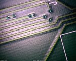
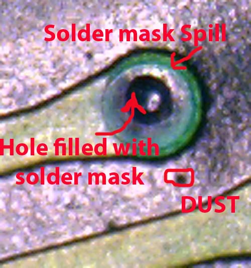
I have a problem with vias opening on my PCBs(Double side only), though i have not opened them in solder mask layer they are opening with reddish copper shade on pcbs.while i asked the same with fabricator he is saying the masking ink is going in the hole when is was placed in hot air level.I have obeserved this with many fabricators.how to eliminate this problem:sad:.If any one of you know, pls share with me
 

1. I don't think, that it must be a problem. Did you check, if the vias are actually exposing the copper, e.g. with a continuity tester. Can you solder the vias?
2. Tenting of vias is treated differently by designers. Also PCB manufacturers have different requirements, depending on their processes. Some processes may be incompatible with tented vias, in this case, the manufacturer will possibly modify the gerber data.
3. I'm not aware of a mask "ink" that will melt during hot air processing, but apparently it exists. Then it's a case of incompatibility with via tenting. I don't know, what's your exact reason to insist on tented vias. If they are essential, you have to look for a manufacturer that uses a different solder mask material.
 

Thanks for you reply


1. I don't think, that it must be a problem. Did you check, if the vias are actually exposing the copper, e.g. with a continuity tester. Can you solder the vias?

means, the colour is like that, when i was checking with meter its not showing the continuity,

2.what's your exact reason to insist on tented vias.

The reason is i want to give my procuct MTBF to 10years, if this is the condition(pls see the attached images), how can i assure that(10years mtbf)..Vias may get damaged due to climatic conditions
 

Attachments

  • 2770-1.bmp
    3.8 MB · Views: 110
  • 1-4.jpg
    1-4.jpg
    1.5 MB · Views: 152

Thanks for providing the photo. I understood the statement about hot air levelling somewhat different before, but it looks like a normal result of solder mask drying. Although solder mask gives some enviromental protection, it's not intended as such, and you shouldn't rely on it. You have to go for conformal coating in case of critical enviromental conditions.
 

Please check the 2770-1.bmp, in the vias are in copper shade, actually vias need to cover with soldermask ink like in 1-4.jpg, but to all pcbs the masking of vias are not coming perfectly.How are your pcbs?could pls show me your pcbs photo(to check whether the vias are fully masked or not?)
 

Making the holes of the vias smaller will decrease this effect. And of course if you worry about the exposed copper you can simply put a white silkscreen on top of every via. Also you can ask the producer to print twice white silkscreen on top of the vias.
 
If i place a white legend in place of via..i may not be able to use that as a test point.why in PCB fabrication the via is not covering with solder mask, what could be the exact reason?

---------- Post added at 08:13 ---------- Previous post was at 07:57 ----------

Ia'm giving 23.62mil(0.6mm) hole, with 40mil(1.016mm) pad for via.To how much extent i can reduce my hole size?my fabricator is saying he can provide up to 12mil hole via with a pad of 20mil. is tehre any problem to signal strength if i reduce the hole diameter of via?
 

Some relaation is there with via size and current carrying ability. You can stich multiple vias insted of a single on for high current traces.
For high frequency traces small vias are prefeered.
12 mil drill size is common and you can go with it.
If you want to use the via as a test point how can you cover it with solder mask?? For the purposes like ICT ( in circuit test) you need vias with mask opening.
 
IF you want to give a 10 year MTBF then do NOT use vias for test points, as doing so can stress the via & cause premature breakdown of the barrel.
Use proper testpoints.

The resist around the via hole is thinner because it flows down the open hole & hence causes the thinning, if you want thicker resist then ask your manufacturer for it
and they can either put it on thicker or double pass it. Or perhaps fill the vias before coating (costs more).

Have you found any evidence that vias like this fail because of the thin resist?

Go with conformal coating. However remember that it keeps stuff in as well as out so the boards need to be clean before coating.
 
Actually the problem you experience is a manufacturing problem . Be sure that if you change the manufacturer probably the problem will vanish. I guess the manufacturer have problems with the solder mask - or it's bad quality, or it was applied not properly or something is wrong during hot HASL process. The via hole size should be as bigger as possible - small diameter vias tend to break and also have problems with bigger currents. I think 0.6mm is normal for a via.

Other way to reduce the effect is to ask for PCB with thinner copper layer which will reduce the difference in the hight between etched and non etched areas. Notice that thinner copper layer also allows to etch thinner tracks, negative side is that it has higher resistance.
 
The vias in the photo shown below seem to be completely covered with soldermask, although the thickness is reduced near the vias. In so far I don's see a problem. I get a similar via look from some manufacturers and didn't see a reason to complain yet.

I don't understand the test point discussion. To use vias as test points, they must not be tented. The shown vias aren't suited as test points in my opinion.
 

In my opinion something is wrong with the vias. The proper soldermask technology uses photoresist solder mask, the photoresist is applied with silkscreen printing and then exposed under UV. What I see is the spills of the soldermask around the vias whcih can happen if they don't apply properly the solder mask (instead of silkscreen they use spraying so liquid soldermask is sucked into via hole because of capilar effects). The hole is also filled with solder mask. There are many dust particles in the solder mask which speak about dusty environment (and probably low quality) -
 

What I see is the spills of the soldermask around the vias whcih can happen if they don't apply properly the solder mask (instead of silkscreen they use spraying so liquid soldermask is sucked into via hole because of capilar effects).
Who defines, that spraying (or wire application) of a soldermask is incorrect? Screen printing can be only applied for low resolution standard technologies. It's legacy at most PCB manufacturers. High resolution can be provided by laminated dry film or liquid resist. The latter will necessarily fill through plated vias and terminal pads, and also have a ring of slightly increased thickness around them, what you call "spill".

There's actually a problem to get the soldermask at untented throughplated holes completely removed. But the finish of tented vias can't be exactly controlled with liquid solder mask.

Dust particles would be another topic. But I can't detect from the photo, if there are actually dust particles. The solder mask seems fully functional.

P.S.: It seems to me, that the said "dust particles" are rather small cavities in the substrate, that absorbed the solder resist.
 

The spills of solder mask around the vias definitely speak about low quality solder mask process. Notice that the precision of the solder mask (how it overlaps the pads) is something different and can't be estimated from this image.

If you look more carefully you'll see many dust particles in the photo. In the high quality PCB there are literally no dust particles at all (and the prices are different of course). During the drying of the solder mask it electrostatically attarcts all dust particles around, so when you see a PCB without dust particles it speaks about really clean environment where special measures were taken to reduce the dust.

>> But the finish of tented vias can't be exactly controlled with liquid solder mask.

I agree if you spray the solder mask or you print it with silkscreen manually the quality can't be controlled. But the quality is compltely different when using silkscreen which is applied with machine (automatic silk screen printers) - the pressure and the speed of the rackel are precisely controlled.

P.S. I would disagree that the "dust particles" on the image are small cavities, I'm inclined to think that the low quality of the solder mask also comes with dusty environment. It looks less possible that they pay huge attention to have clear environmnet and in the same time they do low quality solder mask, usually the low quality is equally spreading on all processes and materials.
 
Screen printing of solder masks achieves a limited position accuracy of about 0.1 mm / 4 mils, so it isn't used by any manufacturer for high resolution SMT PCBs, as far as I'm aware of. Don't want to repeat the other points, that have been already said.
 

yes, its a manufacturing problem.we have intimated to fabricators.The thing started by comparing the PC boards with our PCBS.If you observe in the below link the vias are fully covered with soldermask, and there are no dust particles in the soldermask.In India if there are any fabricator who can cover the via with soldermask, you people pls suggest me.You guys are disussing or giving good points to me.Thnaks for that

https://obrazki.elektroda.pl/29_1294117405.jpg
 

what is the diameter of these via holes? We've had problems with 0.6mm or larger via holes and tenting so the PCB vendor asked us to use 0.5mm (0.4mm is better). If you need higher current capacity then just use more of these smaller vias.
 

Screen printing of solder masks achieves a limited position accuracy of about 0.1 mm / 4 mils, so it isn't used by any manufacturer for high resolution SMT PCBs, as far as I'm aware of. Don't want to repeat the other points, that have been already said.

Actually the photoresist solder mask is applied with silkscreen printing method and then exposed on UV (sometimes they over print 2-3 times the mask to make it thicker and to avoid the silk holes) . The accuracy is extremely high because it depends on the photo process and not on the silk pitch. Before the photoresist soldermask were introduced the solder mask was directly printed with silkscreen but this process was very inaccurate.

The problem is that small PCB factories don't have money to buy automatic silkscreen printers which can only guarantee the even and smooth layer of solder mask photoresist. Instead they print the silkscreen manually which introduces many problems and the quality depends strongly on the operator's skills. Especially with large size boards manual silkscreen printing can bring huge difference in the quality because it requires bigger pressure on the rackel.
 

Ia'm giving 23.62mil(0.6mm) hole, with 40mil(1.016mm) pad for via.This time i will check by reducing the hole size
 

Actually the photoresist solder mask is applied with silkscreen printing method and then exposed on UV
That sounds more plausible. However, none of the major PCB manufacturers I've been working with is using this technique. They are mainly using automated courtain coating machines. I assume, that there are viscosity differences between liquid coating and screen printing material, in so far the finish may look different. But screen printing isn't the industry standard.

I should be also noted, that tented vias are considered distrustful by some manufacturers and professional organisations. They clearly suggest open vias with protective surface finish (HAL or whatever) or a separate via fill process.
 

Status
Not open for further replies.

Part and Inventory Search

Welcome to EDABoard.com

Sponsor

Back
Top