vjabagch
Member level 1
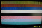
I am working on a DVI controller that will display a color bar pattern on a computer monitor with DVI input.
I have been able to simulate the transmission of the Horizontal Synchronization Pulses and Vertical Synchronization Pulses using Modelsim. In addition I can send out I2C commands through a pullup wire (in simulation only) which will initialize the Chrontel 7301C DVI transmitter chip.
I am using a 100MHz LVDS clock for the input and feeding the signals from the clock into an IBUFGDS (a library component that outputs a single clock signal from the LVDS signal). From this output signal I am deriving a 40MHz signal to serve as the pixel clock for a 800 X 600 monitor at 60Hz. The way I derive the 40MHz clock is through the DCM libary component that realizes clock signals of custom frequencies from an input.
Question 1.
Is it possible run a behavioral or post synthesis simulation on the top level design that has the DCM components in Xilinx so that I can observe the derived clock signal at different frequency (40MHz) compared to the input clock signal (100MHz)? When I behaviorally simulate I only get one type of clock frequency and do not see any difference between the input clock and the pixel clock.
Question 2.
When I attempt to run the design through chipscope I can see constant valued signals but do not see anything changing on the data ports. Though this is unrelated to my first question I need to be able to debug my design at run time. I have actually only seen the constant values without any changes.
I have a clock input set and my data ports set which are considerably slower than the clock input. In fact, the clock input is my pixel clock, which does not even change. Maybe the problem lies somewhere else.
Thank you for taking the time to read the post.
Kind Regards