Continue to Site

Welcome to EDAboard.com

Welcome to our site! EDAboard.com is an international Electronics Discussion Forum focused on EDA software, circuits, schematics, books, theory, papers, asic, pld, 8051, DSP, Network, RF, Analog Design, PCB, Service Manuals... and a whole lot more! To participate you need to register. Registration is free. Click here to register now.

What is the Voltage at Floating node ??

Status
Not open for further replies.

MammPp

Junior Member level 2
Joined
Sep 14, 2008
Messages
22
Helped
0
Reputation
0
Reaction score
0
Trophy points
1,281
Activity points
1,441
Dear All,

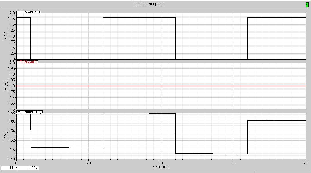
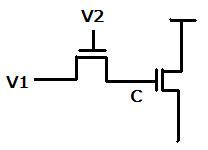
I have some question about floating node. As the following picture,

If I set V1 to be Vdd all the time.
and V2 is Vdd at the first period, then set V2 is 0 (Which is close NMOS)

My question is, what is the value of the voltage at node C ?

and if V2 is zero, the other transistor, which node C is gate of them, is on/off ?

Thank you so much for your help

MammPp

38_1288233081.jpg
 

Hi
Voltage at node C would be V(V1)+q/C, where
q= charge injected by transistor V2;
C= capacitance at node C;
If transistor is of NMOS type than q would be negative - so resultant voltage would be lower than V(V1).
 
  • Like
Reactions: MammPp

    MammPp

    Points: 2
    Helpful Answer Positive Rating
Hi MammPq,

I think that: voltage at node C will be a little bit less than VDD due to the charge injection but enough to keep transistor in the right side on (i. e. VGS higher VT)
 
  • Like
Reactions: MammPp

    MammPp

    Points: 2
    Helpful Answer Positive Rating
Hi all,

Thank you for your answer,

I used HSPICE to simulate this circuit, by consider at V1 and V2 is Vdd.
Let Vdd = 0.9V

The strange result this voltage at node C is equal to 0.13 something, which I concerned that,

From this circuit, if V1 and V2 is Vdd, the other transistor is on/off ?

Moreover, when V2 is off suddenly, voltage at node C is still there or gone ?

and why ???
 

Hi MammPq

1) If V1 and V2 is VDD, so both transistors are ON, and node_C is ~ (VDD - VTH_n). Where VTH_n is the threshold voltage of NMOS.
2) If V1 is VDD and V2 is gnd, so, node_C is a little bit less than (VDD - VTH_n) due to the charge loss. Therefore, transistor in the rigth is still on.

You can check this in my simulations using 0.18 um technology and VDD = 1.8.


I hope the explanation is clear now. If you have other concern, you can post it again.
 
Last edited:
  • Like
Reactions: MammPp

    MammPp

    Points: 2
    Helpful Answer Positive Rating
The figuring of q, is always tricky. Up until the point
that the channel "goes away", the gate charge will
be returned to the (presumably stiff) V1 with the G-S
portion of charge bleeding back at an RC limited rate.

It is not Q=cox*(VH-VL) in the end, because of this.
A charge-conserving model and one well fitted to
(this wafer & lot's) reality is wanted.
 
  • Like
Reactions: MammPp

    MammPp

    Points: 2
    Helpful Answer Positive Rating
thank you for your answer.
It's clear for me now
 

Status
Not open for further replies.

Part and Inventory Search

Welcome to EDABoard.com

Sponsor

Back
Top