Welcome to our site! EDAboard.com is an international Electronics Discussion Forum focused on EDA software, circuits, schematics, books, theory, papers, asic, pld, 8051, DSP, Network, RF, Analog Design, PCB, Service Manuals... and a whole lot more! To participate you need to register. Registration is free. Click here to register now.
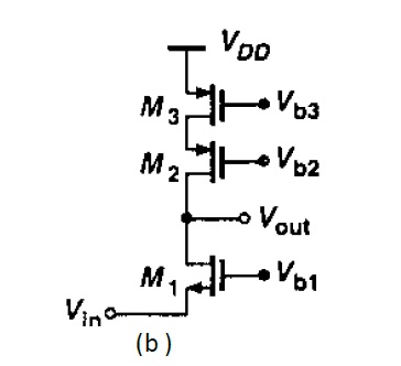
What is the voltage gain, input and output resistances of the following circuit? Ignore body effect and channel length modulation.
I found Rout =1/gm3 but I have doubts about how to find Rin and Av.. Thanks .
You could confirm using small-signal analysis, but the impedance looking into the drain of cascoded MOSFETs is RL = (1+gm2*ro3)ro2+ro3. Replace the two MOSFETs with an impedance with this value. Now you should have a simple common-gate stage where Rin = (RL+ro1)/(1+gm1*ro1)
This site uses cookies to help personalise content, tailor your experience and to keep you logged in if you register.
By continuing to use this site, you are consenting to our use of cookies.