Continue to Site

Welcome to EDAboard.com

Welcome to our site! EDAboard.com is an international Electronics Discussion Forum focused on EDA software, circuits, schematics, books, theory, papers, asic, pld, 8051, DSP, Network, RF, Analog Design, PCB, Service Manuals... and a whole lot more! To participate you need to register. Registration is free. Click here to register now.

Help RF VC Oscillator Design

Status
Not open for further replies.

phriendtj

Newbie level 3
Joined
Nov 15, 2009
Messages
3
Helped
0
Reputation
0
Reaction score
0
Trophy points
1,281
Location
Buffalo New York
Activity points
1,310
I am trying to design an VCO which will work in the range of 88-108 MHz...

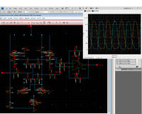
The Problem I seem to be having is that my sine wave is pretty for most of the cycle
but then abruptly jumps...

the output of the source followers is shown in the image below...

of course.. the input looks th same as well...
how do i fix this to get a full clean sine wave?


It's normal... you watch these wavefom single ended and differential oscillators create such waveforms.Because the voltage at each branch rises from zero and reaches to VCC but due to treshold voltages of the output source followers, waveform never drops to exactly zero.Around zero voltage, the MOS is almost OFF ( or weak inversion mode ) and just a leak is seen from the source side due to Cgs.
When you check out this waveform differential, you'll see pure sinusoidal shape.( If the OpAmp is well designed)
 

    phriendtj

    Points: 2
    Helpful Answer Positive Rating
Thanks... I figured it has something to do with the op amp...

it doesn't work so well

it works as a simple noninverting or inverting config for simple amplication.. but when I try to use it as an active low pass filter it falls apart

i went through the design process I found in CMOS Analog Circuit Design by Phillip Allen and Douglas Holdberg...

section 6.3 design of a two stage op amp

the circuit consists of a PMOS current mirror feeding a two NMOS differential amp, with another NMOS tail for current, with the second stage of just two transistors, a PMOS and NMOS

I would post my design, but I am at home now and only have access to cadence at school.. will post later... but any suggestions would be greatly appreciated


any suggestions for improving the Op Amp?

Thanks so much
T.J.
 

Status
Not open for further replies.

Part and Inventory Search

Welcome to EDABoard.com

Sponsor

Back
Top