Continue to Site

Welcome to EDAboard.com

Welcome to our site! EDAboard.com is an international Electronics Discussion Forum focused on EDA software, circuits, schematics, books, theory, papers, asic, pld, 8051, DSP, Network, RF, Analog Design, PCB, Service Manuals... and a whole lot more! To participate you need to register. Registration is free. Click here to register now.

NMOS and PMOS (W/L) aspect ratio versus Vth

Status
Not open for further replies.

allennlowaton

Full Member level 5
Joined
Oct 5, 2009
Messages
247
Helped
3
Reputation
6
Reaction score
3
Trophy points
1,298
Location
Taiwan
Activity points
3,066
hello guys..can help me with this..
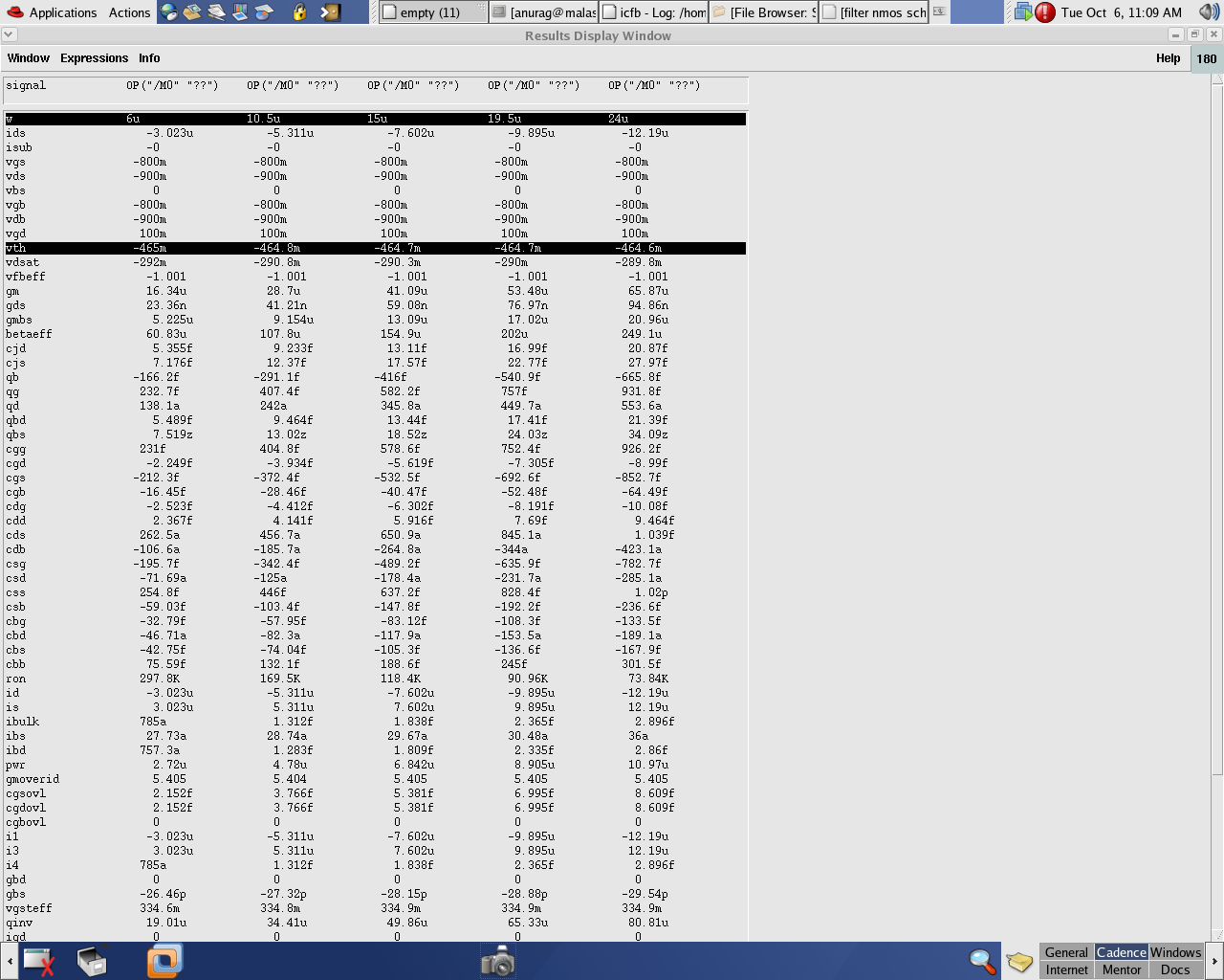
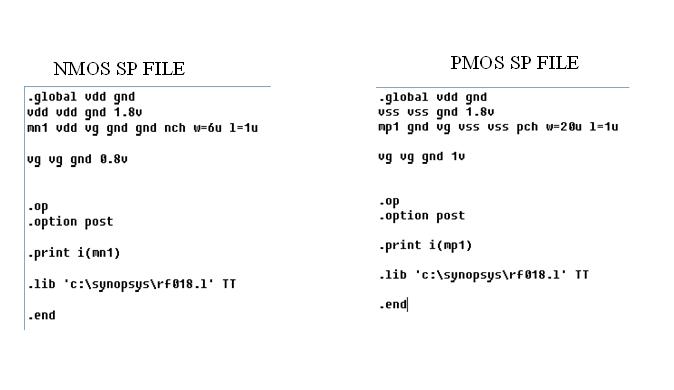
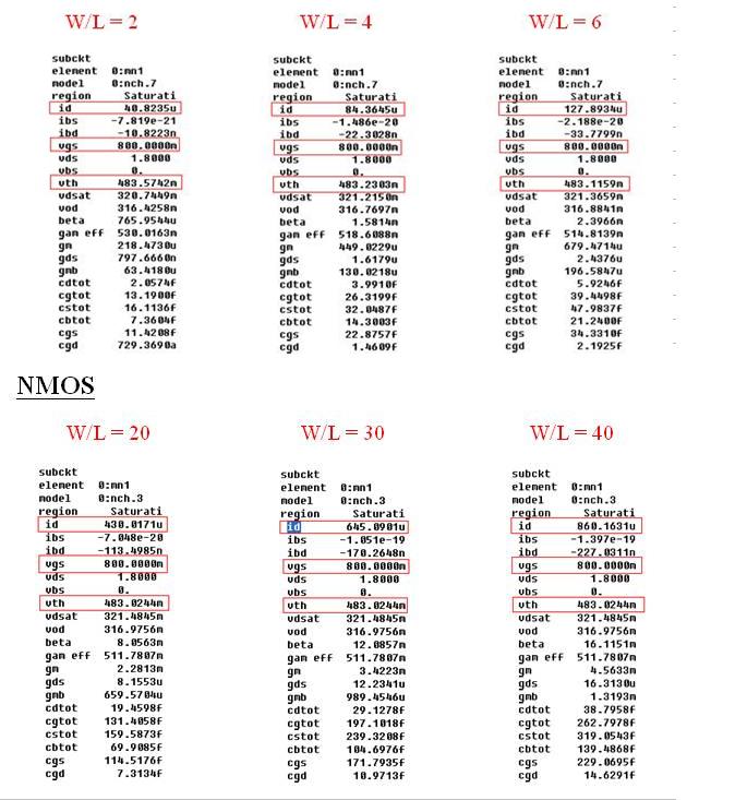
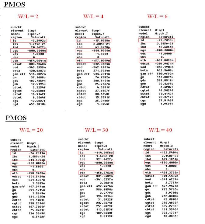
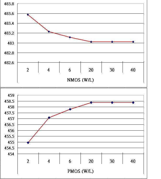
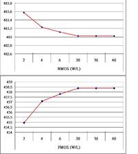
guys please help me explain this..in NMOS: as (W/L) increases, the Vth decreases until it settle to a certain value. while the PMOS: as (W/L) increases, the Vth increases until it settle to a certain value.
The Vgs for NMOs and PMOs are 0.8V.
The supplied Vdd is 1.8V for each of them.
Please to the attachment for more info.
(The values used in the graph is derived from the HSPICE .lis file generated from simulations)


Thank you very much.
 

Phenomena like DIBL will lower the effective VT of
FETs in absolute terms. None of the lengths you show
are likely to see much of this in submicron technologies.

Edge effects may also be a factor, a small region at the
edge is a somewhat effective MOS structure but with some
degraded attributes from strain and oxide / interface
quality. The wider (with W/L) you get, the smaller a part
of the composite device's conduction has to do with that.

Delta-W from lithography may be positive or negative.

Now you have to distinguish between what happens in
the simulator, and reality. Some of the numbers seem
like "who cares?" kind of small differences, and the more
"interesting" behavior lies to the left of charted values.
It would not surprise me if all this were simply fitting
artifacts.

I would blithely ignore a millivolt VT difference since I'm
used to seeing 5mV-range mismatch on identical ones.
 
Thank you very much for the reply sir/madame.

But still I'm still confused why the NMOS's Vth decreases and the PMOS's Vth increases given their aspect ratio being increased?

I'm trying to relate this observation to the calculation of the aspect ratio in my future design of devices using the CMOS.

I know, the variations of the Vth is negligible to take into account. But I just want to satisfy my curiosity. Hope, anyone of you guys can help me.

Thank you once again.
 

Hi,
I did ran the simulation for PMOS to get Id vs Vds. For L= 6u and W = 6u to 24u and I saw that Vth was decreasing with increasing W/L. Check the attached image.

 
Thank you zopeon for your help.
Our results are contradicting with each other.
In my case, I'm using a constant L=1u in all of the widths.
Please refer below for my .sp files for PMOS and NMOS. I supplied Vg=1v in the PMOS so that it can have Vgs=-0.8v just like the Vgs=0.8 for the NMOS in this simulation.


Added after 9 minutes:

Here are the result of simulations for NMOS
Please refer below.


Added after 56 seconds:

Here is the result for my PMOS


Hi allennlowtown,
I tried doing with L =1um and the vth did increase for increasing W, So I guess its short channel effect, but I am concerned about short channel effects at even 1um length for 180nm node! But I dont know which effect is causing the change. Perhaps someone with device modeling background could explain?
 
wow..thank you very much once again zopeon. You had exerted a lot of effort with this already. Maybe I will also make some simulations using the 0.18um as length but with aspect ratio being retained.
 

Status
Not open for further replies.

Similar threads

Part and Inventory Search

Welcome to EDABoard.com

Sponsor

Back
Top