ronydc
Full Member level 3
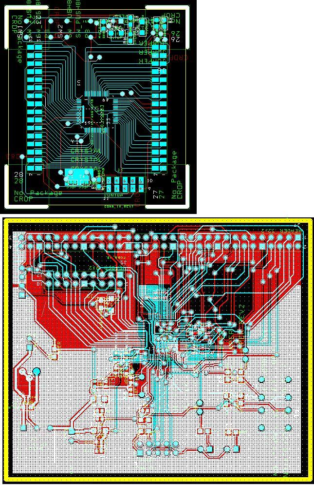
jumper orcad
DEAR FRIENDS,
SINCE quite a long.. i m been trying to design a simple single sided pcb in ORCAD.
BUT its not working..!!
I AM quite used to with the software .. but its unable to design a single side pcb ..!!
any how it keeps some 3 nets unrouted..!!and THERE IS NO FACILITY IN THE SOFTWARE ( I FEEL SO) THAT WE CAN MANUALY DRAW A TRACK..!!
EVEN I AM UNABLE TP PUT THE JUMPERS FOR The 3 nets it lefts behind..!!
whts the use of this dull softeware..!!!
I m now fed up with this kinda softwares..!! most of this kind of softwares cant design SINGLE SIDED pcb...!!
and if thay cant make a pcb for single sided by auto routing , thy dont have facility that we can make a track by ourself ..!!!
can some EXPERT show me the guideline .?
--ROny..!
NOTE : PLEASE I aM IN BaDLY NEED TO DESIGN some PCB'S. so help me ..!!