Continue to Site

Welcome to EDAboard.com

Welcome to our site! EDAboard.com is an international Electronics Discussion Forum focused on EDA software, circuits, schematics, books, theory, papers, asic, pld, 8051, DSP, Network, RF, Analog Design, PCB, Service Manuals... and a whole lot more! To participate you need to register. Registration is free. Click here to register now.

Running AutoRoute for Overnight?

Status
Not open for further replies.

umery2k75

Advanced Member level 1
Joined
Apr 19, 2006
Messages
434
Helped
41
Reputation
80
Reaction score
15
Trophy points
1,298
Location
Pakistan
Activity points
5,748
best pcb autorouter

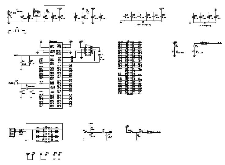
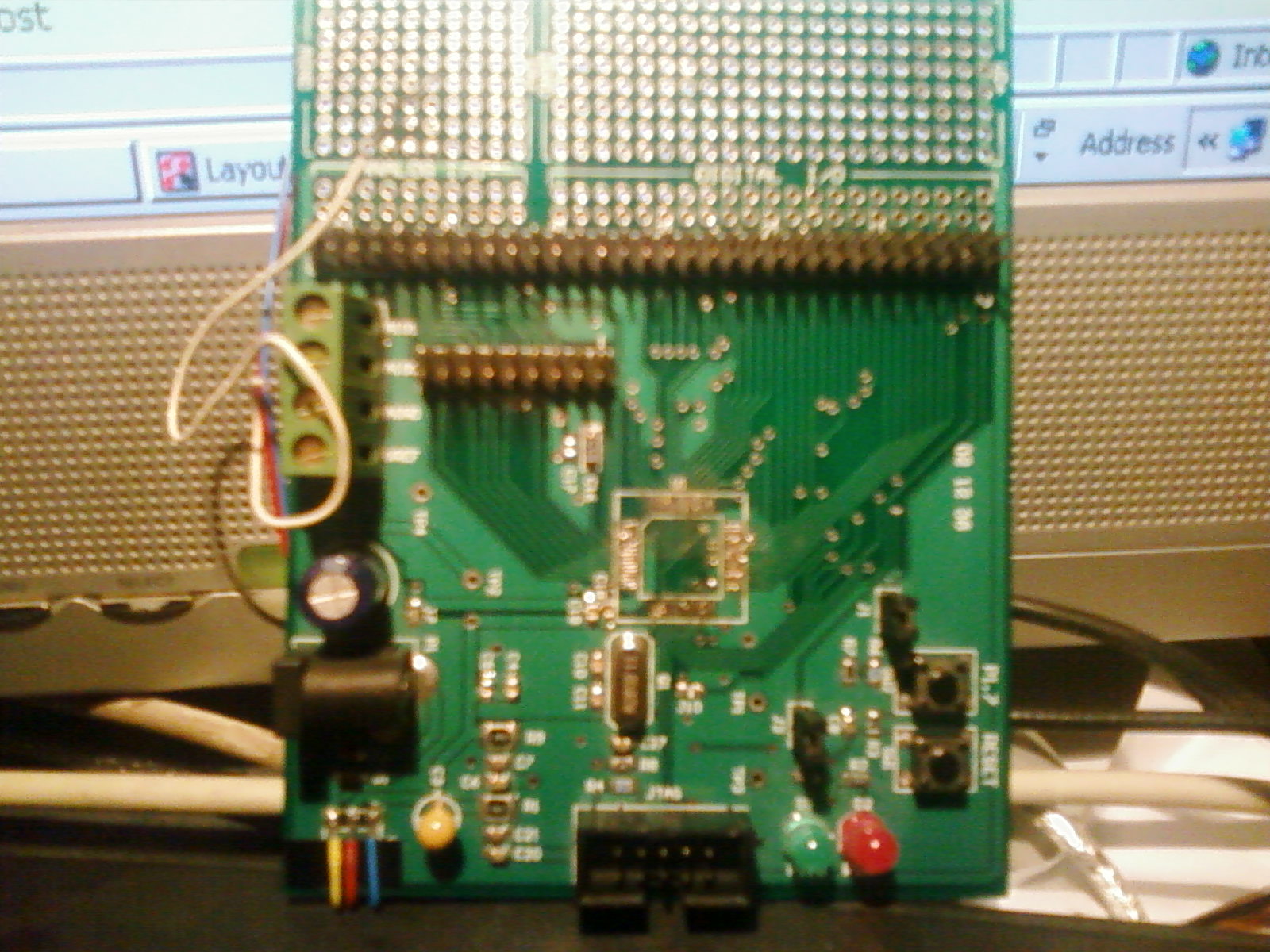
I'm not able to completely autoroute the PCB using Orcad 10.0 Layout Plus. I have tried so many things to be able to route the PCB, but I'm not able to get through.
If you look at the URL below:
https://www.orcad.com/forums/ShowPost.aspx?PostID=11022
then you'll find saying
A good designer can route a lot more efficently than any autorouter. They are getting better and they do save time if you set them up to run overnight
Orcad autorouter doesn't work for more than 1 minute, then it gives message "All sweeps completed( or disabled) ", how come people run this software overnight. Computer keeps on trying and trying and trying......
 

autoroute in orcad

Have you tried looking up the Help documents of OrCAD for this error?
As always, manual routing is always better than auto routing, especially for critical nets.
 

top autorouters

Yes, I'm still looking at the documentations.
 

autorouting orcad 10.0

Hi,

How big is your board? How many nets? components? Topology?
Why you need to Auto route?
OrCAD Auto Router is not a very capable tool. Even with some of the best Auto Routers like Specctra you wont always get the desired results the first time. Remember the saying "Auto Router is as intelligent as the person who sets it up"

M
 

best pcb autorouter

93_1233860664.jpg

Only this big and physically it's small.
 

best autorouter

Design seems pretty simple... Check your placement if you can optimize your pin out.
How many layers have you assigned? Any PWR planes, via sizes and grids.
Having said that I will not use Auto Router for this simple design...It should take you maximum of few hours to do a nice clean route manually.
 

autoroute pcb


This is the board, if you see the tracks of the middle IC. I had accidently damaged it, so getting a new PCB will take much time. I believe I can make this PCB at home too, so I can start doing work again.I talked to local PCB maker, he said how many piece you want 100,200. He wasn't willing to do a one piece even of 2 layers, it will cost very high. I already know about the placements of this board.I am using only 2 layers, top and bottom. I don't know this PCB is of how many layers? I think it's of two layers. Because today, in the morning I took this PCB in my hand and tries to see the SUN through it. I was trying to see the tracks beneath the PCB.I didn't find any track or any shade beneath the green board. Sun light seems to penetrate it. I don't know if this method of judgement is correct or not, about checking layers of PCB. It's one of my keen wish to design a PCB of more than 2 layers. Locally we don't have any company over here making PCBs of more than 2 layer.So even if I want to make one for experment, I have to give order to another country.

Added after 1 minutes:

I am doing manual routing.
 

all sweeps completed (or disabled)

Is hard to say from pic. but if I had to take a guess I would say is a 4 layer board.
You have two GNDs on your schematic and looks like they have used plane on top to connect one of them. If you copy the same placement it should be OK. Also ask the company where you got this evaluation board if they can send you Gerbers for it. Some company will do this. There are some quick turn PCB shops on line where you can get two to four boars very cheap price. Contact them first, usually they have their requirements which you have to follow to get their base price.

M
 

    umery2k75

    Points: 2
    Helpful Answer Positive Rating
best autoroute pcb

Thanks for such nice information.
1) I didn't know about the quick turn PCB shops on line.
2) I didn't know if there are companies out their sending gerber file.

I'll try them out for sure. I have seen these VIAs on my board, on the board they appear as irregular copper pour layers.

25_1234278863.jpg


As it's night, so I tried to see through the board from a bright lamp.Again I can't see tracks beneath the PCB. I don't know if this practice is correct or not. To prove this technique, I will do the same practice to see through the boards of other SMD PCBs. I have an old graphics card 32MB Nvida, I'm sure it must be more than 2 layers and some HDD Hard Drive PCBs and others PCBs I might have. I'll check all of them.
 

orcad autoroute technique

I have seen these VIAs on my board


Those are TPs for probing. One per each PWR and Return (Analog and Digital).

Good Luck,

M
 

    umery2k75

    Points: 2
    Helpful Answer Positive Rating
best auto route

TPs=Test Point?
But why would any one put test point of such things on the board? Equipped with an Oscilloscope what's the most, a person could get from it? Just to check out voltage level and to see if there's any ripples in it or not.
 

autoroute 4 layers

PWRs and GNDs are some of mostly probed nets. I put minimum three per each PWR /GND and scatter them on board. In general for debugging is good to have GND access in different parts of board.

If you have board that used in production then ICT method is preferable provided if there is enough space to get access to majority of nets.

M
 

    umery2k75

    Points: 2
    Helpful Answer Positive Rating
Status
Not open for further replies.

Part and Inventory Search

Welcome to EDABoard.com

Sponsor

Back
Top