Continue to Site

Welcome to EDAboard.com

Welcome to our site! EDAboard.com is an international Electronics Discussion Forum focused on EDA software, circuits, schematics, books, theory, papers, asic, pld, 8051, DSP, Network, RF, Analog Design, PCB, Service Manuals... and a whole lot more! To participate you need to register. Registration is free. Click here to register now.

Question about the switch cap in VCO design

Status
Not open for further replies.

gaom9

Full Member level 4
Joined
Oct 8, 2007
Messages
228
Helped
7
Reputation
14
Reaction score
5
Trophy points
1,298
Location
China
Activity points
3,294
Hi,
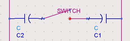
I am designing a VCO and using the switch capacitor to change the VCO output frequency range.
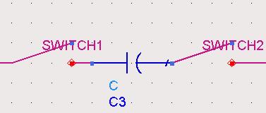
I have a question about the switch capacitor array. I have read some paper about the VCO design, and the circuit they used for switch capacitor is as Figure 1, which contain two capacitor and one switch, but why do they use the circuit as shown in Figure 2, which contain one capacitor and two switches?
As the circuit in Figure 1, the equal value of the capacitor is only a half of one capacitor, and it will cost twice layout area.
Is that because of the capacitor quality factor? As the MOS switch will introduce some resistance to the circuit, so we should decrease the number of switch?

Can anyone give me some advice about this, please?
What is the difference between the two circuit in Figure 1 and Figure 2?


Thank you!
Best regards!


65_1222912265.jpg

19_1222912290.jpg
 

To improve the Q of capacitor array! There is more resistor series than figure1 if the switch is same each other.

Higher Q of capacitor array is better for VCO.
 

    gaom9

    Points: 2
    Helpful Answer Positive Rating
Thank you for your reply.

I try this two kind of circuit, the circuit of Figure 2 will make the VCO work badly.

But how to design the MOS switch size to ensure Q of the capacitor?

Thank you!
Best regards!
 

gaom9 said:
Thank you for your reply.

I try this two kind of circuit, the circuit of Figure 2 will make the VCO work badly.

But how to design the MOS switch size to ensure Q of the capacitor?

Thank you!
Best regards!

You know there is parasitic capacitor and parasitic resistor of switch, and they are both bad for VCO design.
So must trade off between them.

First, we should use the minimum length, then larger width will be lower resistor, but larger parasitic capacitor. And larger parasitic capacitor leads to lower tuning range.

But if the tuning range of VCO is enough, you should increase the Width of switch.

Besides, the width of switch should be in direct proportion to the capacitor value.

For example, 10/0.18 for 0.4p capacitor, then 20/0.18 for 0.8p capacitor. Then generate a capacitor array.
 

    gaom9

    Points: 2
    Helpful Answer Positive Rating
Thank you for your reply, jecyhale.
Your reply provides some key information for my design.
Especially "the the width of switch should be in direct proportion to the capacitor value", I used the same switch width for different capacitor before.
I will try again.

Thank you!
Best regards!
 

gaom9 said:
Thank you for your reply, jecyhale.
Your reply provides some key information for my design.
Especially "the the width of switch should be in direct proportion to the capacitor value", I used the same switch width for different capacitor before.
I will try again.

Thank you!
Best regards!

Welcome.

I think we should ensure all parasitic capacitor should be twice and the Q of capacitor+switch should not change when the value of capacitor increase to twice.

In other words, no matter what the capacitor is, the Q does not change.
 

I am using switch capacitor bank in my VCO design, with C,2C,4C,8C values. I used unit capacitor architecture, for example putting 4 Capacitors in parallel to make 4C value. Is it degrading the Q factor and should I use a single 4C cap value instead of it?
 

Perhaps I'm missing something but the first array with two caps and one switch means the switch is floating. I would think that would be susceptible to stray charges and undefined voltages on the node.
 

Status
Not open for further replies.

Similar threads

Part and Inventory Search

Welcome to EDABoard.com

Sponsor

Back
Top