Continue to Site

Welcome to EDAboard.com

Welcome to our site! EDAboard.com is an international Electronics Discussion Forum focused on EDA software, circuits, schematics, books, theory, papers, asic, pld, 8051, DSP, Network, RF, Analog Design, PCB, Service Manuals... and a whole lot more! To participate you need to register. Registration is free. Click here to register now.

question about rail to rail input/output amp

Status
Not open for further replies.

stephenho

Newbie level 4
Joined
Oct 31, 2007
Messages
6
Helped
0
Reputation
0
Reaction score
0
Trophy points
1,281
Activity points
1,316
Could you please tell my how to set DC voltage level of drain of M16 and M14?

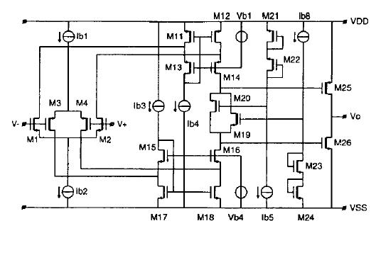
This is a rail to rail input and output amplifier and its constant-gm control circuit is omitted.
M25 and M26 are class-AB output transistors.Threshold voltage are -0.65V and 0.73V, respectively.And VDD is 3V.

So,my question are:
(1) what is exact DC voltage for the drain of M16 and M14?
(2)if DC voltage of the drain of M16 and M14 are already made certain,how to set DC voltage level of drain of M16 and M14?

Thank you all, wish you good luck.This is the first quesiton of mine.
 

What I understand form the schematic
is that the M14 and M16 are the cascode devices.
These two are driving the class A-B output so ..

.. at Max VDRAIN(M14) = VDD - | Vtp |
.. and Min VDRAIN(M16) = Vtn

Other limits will be according to swing specs , i suppose ..

Regards
Raduga
 

    stephenho

    Points: 2
    Helpful Answer Positive Rating
M11-M18 compose the cascade current mirror load. According to the type of the cascade current mirror:
The maximum drain voltage of M14 is VDD-2*VODp, where, VODp is the over drive voltage of PMOS.
And the mimimum drain voltage of M16 is 2*VODn, where, VODn is the over drive voltage of NMOS.

The actual drain voltage of M14 and M16 is determined by the bias current and the size of M19 and M20. The drain voltages of M14 and M16 should be separated enough to ensure that M25 and M26 do not conduct simutaneously when no input signal.
 

    stephenho

    Points: 2
    Helpful Answer Positive Rating
I have implemented this circuit(I mean Class-AB outout stage and summing circuit).
M19 and M20,the mesh transistors,compose a "floating voltage source".
Voltage difference between M19's source and M20's source is 1.137V in my circuit and quiescent currents flow through M19 and M20 are 7.5uA.

But, when a small voltage signal is applied on gates of complementary input transistors, there is still voltage sine vibration between M19's source and M20's source,and magnitude is about 1mV.

If anyone knows something about this circuit,PLZ tell me.I appriate the help.
 

But why do you wonder from this? There are must be a voltage variation bw sources M19 and M20. This voltage variation is Uinp*Gm*[1/(gm19+gm20)], here Uinp - input voltage on gates of complementary input transistors, Gm - transcondactance of the input complementary differential pair, gmn - transcondactance of each M19 and M20.
 

    stephenho

    Points: 2
    Helpful Answer Positive Rating
in which ic number rail to rail operation avilable
 

    stephenho

    Points: 2
    Helpful Answer Positive Rating
Status
Not open for further replies.

Part and Inventory Search

Welcome to EDABoard.com

Sponsor

Back
Top