Continue to Site

Welcome to EDAboard.com

Welcome to our site! EDAboard.com is an international Electronics Discussion Forum focused on EDA software, circuits, schematics, books, theory, papers, asic, pld, 8051, DSP, Network, RF, Analog Design, PCB, Service Manuals... and a whole lot more! To participate you need to register. Registration is free. Click here to register now.

2 stage CMOS amplifier with lead compensation CM range

Status
Not open for further replies.

Crusader370

Junior Member level 1
Joined
Jun 19, 2006
Messages
17
Helped
0
Reputation
0
Reaction score
0
Trophy points
1,281
Location
montreal, canada
Activity points
1,425
Hi All,

We are doing this project at school, and we are going crazy.

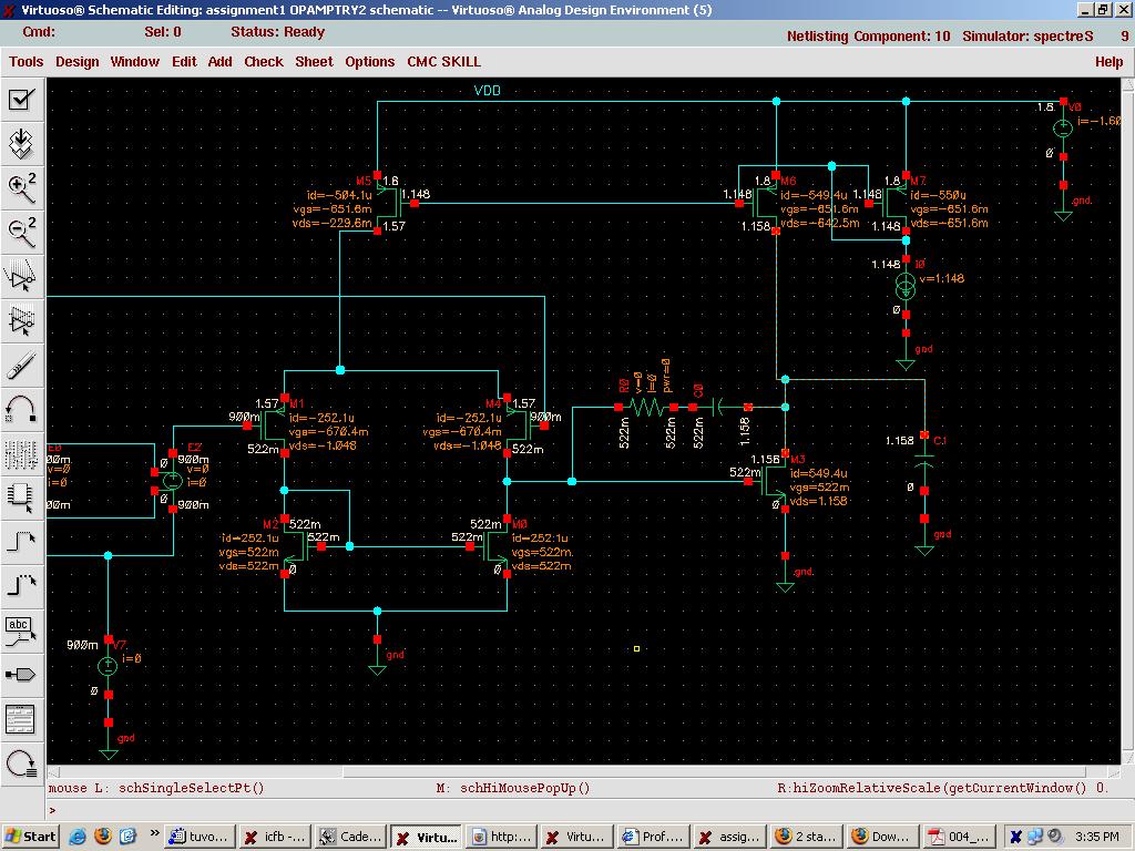
Does anyone have any experience with the following circuit:

**broken link removed**

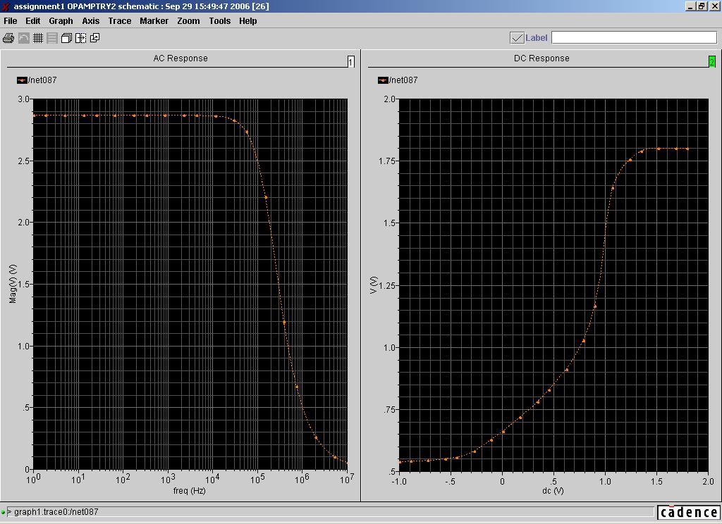
Our biggest problem is our input and output common mode range, as you can see here:

**broken link removed**

Now, this CM DC sweep was done with transistor sizes much larger than on the shown schematic, and when they are reduced in size, it improves, but still, there is that low-slope region on the left, which we can't get rid of. No matter what we try... it won't work...

Any ideas?

Thanks,

Crusader
 

Low gain means that some of active components does not work in active region...
If you are not sure which plot vds voltage of all transistors and see if Vds (Vsd for pmos) drops below Vdsat=200-300mV.
I think that your mirror transistors are too small i.e Vgs is too high and that you have problem with left mos of differential pair. Try to increase W/L of differential pair current mirrors.
 
The W/L of all transistors when the DC sweep was done was very large (500-1000), so I don't think that was the problem. Theoretically, if W/L is large, that would mean that Vov is small for the same current, and therefore the voltage swings would be high... not low... No idea what's wrong.
 

Crusader370 said:
The W/L of all transistors when the DC sweep was done was very large (500-1000), so I don't think that was the problem. Theoretically, if W/L is large, that would mean that Vov is small for the same current, and therefore the voltage swings would be high... not low... No idea what's wrong.
Take from analogLib idc and set dc current to 250u (or 500uA)
copy only diode connected nmos from current mirror and connect idc from vdd to drain. How much is voltage at the drain?
If it is too high W/L should be increased...
Differential pair transistors should be designed to have higher W/L than current mirror transistors.
For good matching L should be 4-5x Lmin... In which technology do you work?
Can you print dc voltages?
 
Will do, as soon as I get to uni today... this will be a loooong weekend with few hours of sleep :(

Technology: 0.18u
 

Crusader370 said:
Will do, as soon as I get to uni today... this will be a loooong weekend with few hours of sleep :(

Technology: 0.18u
Dont worry its easy...
You have this ampliifier in every analog book (for example Phillip-Allen's book)
 
DC voltages:

86_1159558506.JPG


However, in the specification, it says that the input CM should be 0.9V. Now, if I introduce the offset voltage at the input to make the output voltage 0.9V, won't that violate the specification? Some people have been telling me to do this.

Added after 13 minutes:

The ac and dc analysis of the above circuit is:

70_1159559354.JPG


Notice how the input CM range is very low.

Added after 15 minutes:

"Differential pair transistors should be designed to have higher W/L than current mirror transistors. "

Could you explain why?
 

dc biasing is ok.
Try to make larger output nmos to produce lower voltage...
ac response is not good.
At which generator has you put ac amplitude?
 
The ac input is 1mV, so our gain is almost 2900... In our specifications, we need a gain of 60dB, or 1000.
 

Than it is ok . Plot phase response and see phase margin.
If you put 1v you can see gain (2900) directly...
Where is the problem. Can you post your specificatuions?
 
the problem is in the CM input and output ranges

My specs are:
- DC gain > 60 dB (maybe a typo... I am assuming this means the AC gain.. maybe he meant DM gain)
- unity gain bandwith > 170 MHz
- slew rate > 150 V / us
- settling time within 20ns (withing 0.4% of the final value)
- input and output swings of at least 50% of the supply full scale
- input referred RMS noise is less than 1mV
- minimum static power dissipation

Load capacitance: 1.5pF
CM input voltagle: 0.9 V
Power supply: 1.8 V

By the way, I am not sure if I am measuring the input referred RMS noise correctly. I do a "noise" analysis, plot the "equivalent input noise" and then square the line, integrate, divide by the frequency range (not sure about this), and then take a square root.

Added after 3 minutes:

And the current in the ideal current source was determined such that the slew rate specification is satisfied.
 

Crusader370 said:
the problem is in the CM input and output ranges

My specs are:
- DC gain > 60 dB (maybe a typo... I am assuming this means the AC gain.. maybe he meant DM gain)
- unity gain bandwith > 170 MHz
- slew rate > 150 V / us
- settling time within 20ns (withing 0.4% of the final value)
- input and output swings of at least 50% of the supply full scale
- input referred RMS noise is less than 1mV
- minimum static power dissipation

Load capacitance: 1.5pF
CM input voltagle: 0.9 V
Power supply: 1.8 V

By the way, I am not sure if I am measuring the input referred RMS noise correctly. I do a "noise" analysis, plot the "equivalent input noise" and then square the line, integrate, divide by the frequency range (not sure about this), and then take a square root.

Added after 3 minutes:

And the current in the ideal current source was determined such that the slew rate specification is satisfied.

-DC gain you determine from ac analysis at low frequencies...
it is 2900-
-dc swing you can determine if you make buffer- connect minus input node to output(disconnect voltage source from minus) and do sweep at plus node from 0 do Vdd. It works well in the range where output voltage is equal to input.
-Slew rate should be OK
-noise
total rms output noise=rmsNoise(0.1, 20G)
Equivalent input rms noise calculate when divide total rms at output by dc gain and see if it is less than 1mV. If not increase differential pair, decrease nmos mirror.. You can divide it by sqrt(bandwidth) to get equivalent input noise density (v/(sqrt(Hz)) )
-slew rate can calculate from miller C and gm of output nmos...
Then you can see how much current do you need...
-Set phase margin at 60-70 degrees to get settling time...


You can send me pm if you have more questions.
 
Hi Crusader,
If u still havent solved the problem...then try checking for systematic offset in op-amp. The DC sweep is typically the curve one would obtain if the systematic offset is not zero. Also, the DC curve you have shown is swept from negative range...when the supply is single (Vdd) how can you sweep on the negative side...remember negative side it is GND.

regards
 

I suggest you can add a NMOS source follower in front of gate of M3 to buffer the output of first stage. And check the DC and AC again.
 

I have quesstion here

I have same project, I want your help
 

Status
Not open for further replies.

Similar threads

Part and Inventory Search

Welcome to EDABoard.com

Sponsor

Back
Top