Continue to Site

Welcome to EDAboard.com

Welcome to our site! EDAboard.com is an international Electronics Discussion Forum focused on EDA software, circuits, schematics, books, theory, papers, asic, pld, 8051, DSP, Network, RF, Analog Design, PCB, Service Manuals... and a whole lot more! To participate you need to register. Registration is free. Click here to register now.

Dead time calculation in dual active bridge converter

Status
Not open for further replies.

abhishek.2138

Full Member level 2
Joined
Dec 21, 2013
Messages
131
Helped
0
Reputation
0
Reaction score
1
Trophy points
1,298
Activity points
2,383
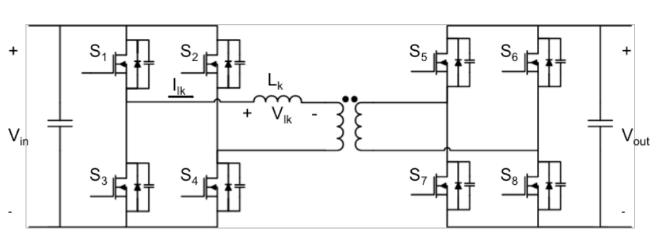
How to calculate the dead time in dual active bridge converter?

MOSFET ON time = 70ns.
Frequency = 100 kHz.
Duty cycle = 50%.
Magnetizing inductance = 720uH
Leakage inductance = 22uH
Input DC voltage = 800V
Output DC voltage = 450V

Pls refer reference schematic.

DAB.png
 
Last edited:

Hi,

the given values have minor impact on dead time (requirements)

More important are the MOSFET parameters and the gate driver parameters.

MOSFET manuafcturers as well as gate driver manufacturers usually provide very good application notes about this topic. Please go through some of them.

Klaus
 
Thanks KS,
Actually, I am looking for derivation.
Can you pls suggest some clues to derive equation...
 

Hi,

I already told you:
I don´t have every formula in mind.
So, if I had to do the job: I had to read the application notes.

This is my way. You are free to do it the same way or not.

Klaus
 
Well...you shoudl best wait for the VDS of the FET to go to zero before switching on......so the peak magnetising current is your current (plus whatever contribution you also get from the resonant inductor current....the capacitance you must charge/discharge is equal to 2 * CDS.......then you have dt = L.di/v
where v is the bus voltage.

So there you have it. If not, start with 200ns dead time and see if it gives you near zero voltage switch_on or not.
 
Be careful with the definitions of the timing numbers you
will use. Switching time may be the 50%-50%, rather than
the "reached zero" you'd probably prefer. You might also
care about details like driver prop delay and drive current
asymmetry when you're playing opposite switching
directions against each other.

I would favor a realistic simulation (if realistic switching
models can be had) because timing will follow Iload and
Vin to some extent (finite driver current, varying charge).
You might find, if your conditions range widely enough,
that you want "adaptive dead time" (meaning, forget a
single point closed form solution).
 
  • Like
Reactions: d123

    abhishek.2138

    Points: 2
    Helpful Answer Positive Rating

    d123

    Points: 2
    Helpful Answer Positive Rating
Hi
This is like synchronous phase-shift topology.
The deadtime has been design for 02 main purposes:
  1. Not make short circuit when 02 Mosfet on one branch not close fully (in trasistion time). This make spike high current in very short time, make Mosfet's temperature higher and go to spoil.
  2. Duty is never 50% - 50%, mean un-balance current when "charge and discharge". Repeat many time, maybe "charge" current rise up > "discharge" current. This make flux in core of transformer run to saturation point. And short circuit will happen - Boom ... ! So, the real Duty+ (high side) and Duty- (low side) need to calculate/setup/config in firmware/hardware have to ballance most if can Duty+ ~= Duty-. Hardware is hard to change, but it normally devided by fipflop so no need care so much. For firmware, should select Center Edge Align mode. Deadtime will add to each duty on and off. Have to check with oscilloscope to ensure. Dead time need long enough to reset flux in core. This follow how much different between Duty+ & Duty- or load when Duty+ & Duty- balance or not. If Deadtime too long, will lost ZVS condition, make Mosfet hotter, lost efficiency.
So, check real condition, with driver, mosfet, transformer, load in secondary side.
I don't have formular, thus check real condition.
Many thing very simple but make Power Electronics go to "Art". If using IC driver, highside driver signal often delay ~50ns to low side... -> optimize driver (synchronous driver signal timing) easy for single for few pcs prototype, but will not good for mass production. Select carefully deadtime for each combo Mosfet + Driver + Frequency.
 
...Yes, though i think with suitable primary current limiting, it would not be possible to get saturation of the transformer due to improper dead time setting. Whether using DAB or PSFB, or whatever.
The attached is a PSFB sim (LTspice) to play with dead time, if the OP wants.
 

Attachments

  • PSFB_5500W.zip
    4.4 KB · Views: 120

Hi
Simulation is not real, the transfer function of transformer is too sample. It is defined base on gain from inductance of two coils.
You can take a look about Remanence or remanent magnetization or residual magnetism.
It will happen near B_peak close B_max, when system near overload or control loop is not stable.
As temperature become higher B_max of core will reduce.
It maybe similar this picture:
Yes, in most case, don't care. Like LLC have serial capacitor will "lock" dc current, not fear saturation.
1667279677750.png
 

Dead time is not strictly calculable due to the non linear capacitance of the mosfets usually used, if one assumes a capacitance Cfet1 + Cfet2 ( the cap of the fets in the totem pole is additive ) = 1nF

Then for a given current in a driving fet at turn off, say 20A, i/C = dv/dt

if the rail to be traversed is 700V say then dt from the above is 35nS - this is the required dead time for this particular operating point

As may by now have dawned on you - the optimal dead time varies with turn off energy in the leakage or other series inductance, (which is also current at turn off ) - and rail voltage.

If you arrange for excess energy then you get extra allowable dead time before the voltage rings away from the rail ...

more questions ... ?
 

Status
Not open for further replies.

Part and Inventory Search

Welcome to EDABoard.com

Sponsor

Back
Top